
Activation chamber and kit used in treatment device for lowering electron affinity, treatment device that contains said kit and is used to lower electronic affinity, photocathode electron-beam source, electron gun containing photocathode electron-beam source, free-electron laser accelerator, transmission electron microscope, scanning electron microscope, electron-beam holography microscope, electron-beam lithography device, electron-beam diffraction device, and electron-beam scanning device

a technology of activation chamber and kit, which is applied in the direction of electron gun containing photocathode electron beam source, electron-beam scanning device, electron-beam lithography device, etc., can solve the problems of lowering the capability of the electron gun, affecting the operation of the device, so as to reduce the scale of the device, improve the ease of manipulation of the existing electron gun, and improve the effect of the ability to manipulate the existing electron gun

Active Publication Date: 2016-06-16
PHOTO ELECTRON SOUL INC
View PDF9 Cites 6 Cited by
  • Summary
  • Abstract
  • Description
  • Claims
  • Application Information

AI Technical Summary

Benefits of technology

The present invention provides a device for surface treatment using a vacuum chamber and an electron-beam source. The device can be smaller and easier to manipulate compared to existing devices. It can be used in existing electron guns or other devices without the need for a new chamber. The electron-beam source can be used in various devices to achieve reduction in size, improved ease of manipulation, and improved functionality. The technical effects of the invention include improved efficiency and convenience in surface treatment and reduced device size and cost.

Problems solved by technology

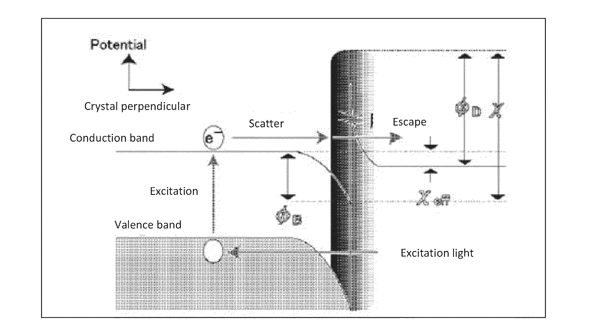
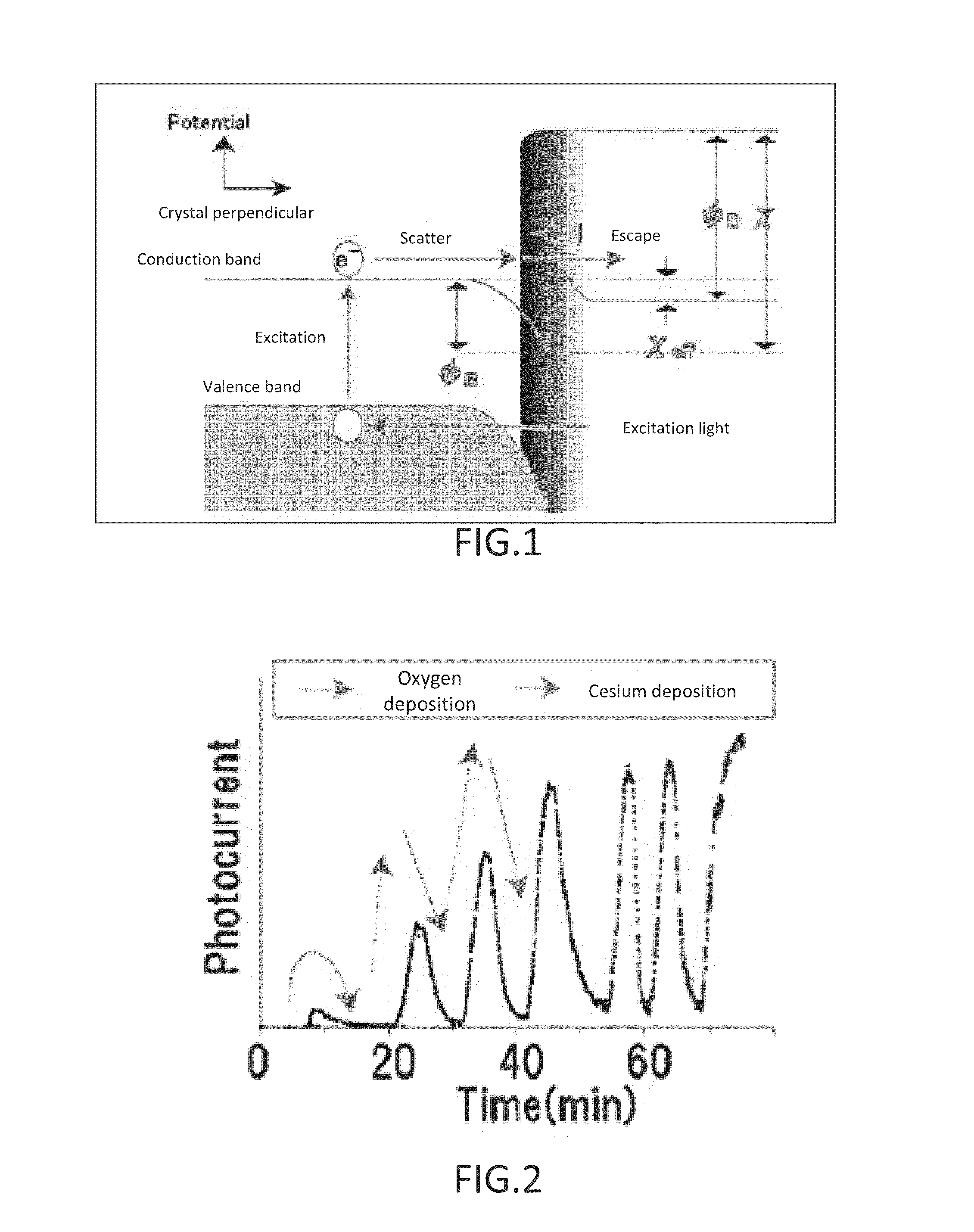
Moreover, even after treatment to bring the photocathode to the NEA surface state, continued emission of electrons may in some cases lead to electrons being emitted while the energy level of the vacuum level of the photocathode returns to a high level from a level lower than the energy level of the conduction band.
The reason was that in conventional EA surface treatment there is adopted a method involving vapor deposition of a surface treatment material directly onto the photocathode inside a chamber, but when EA surface treatment is carried out in the same chamber, the EA surface treatment material is deposited onto the electron gun chamber and various devices inside the chamber, and EA surface treatment material deposited near the electrodes in particular can lead to the occurrence of field emission dark current, dramatically lowering the capability of the electron gun.
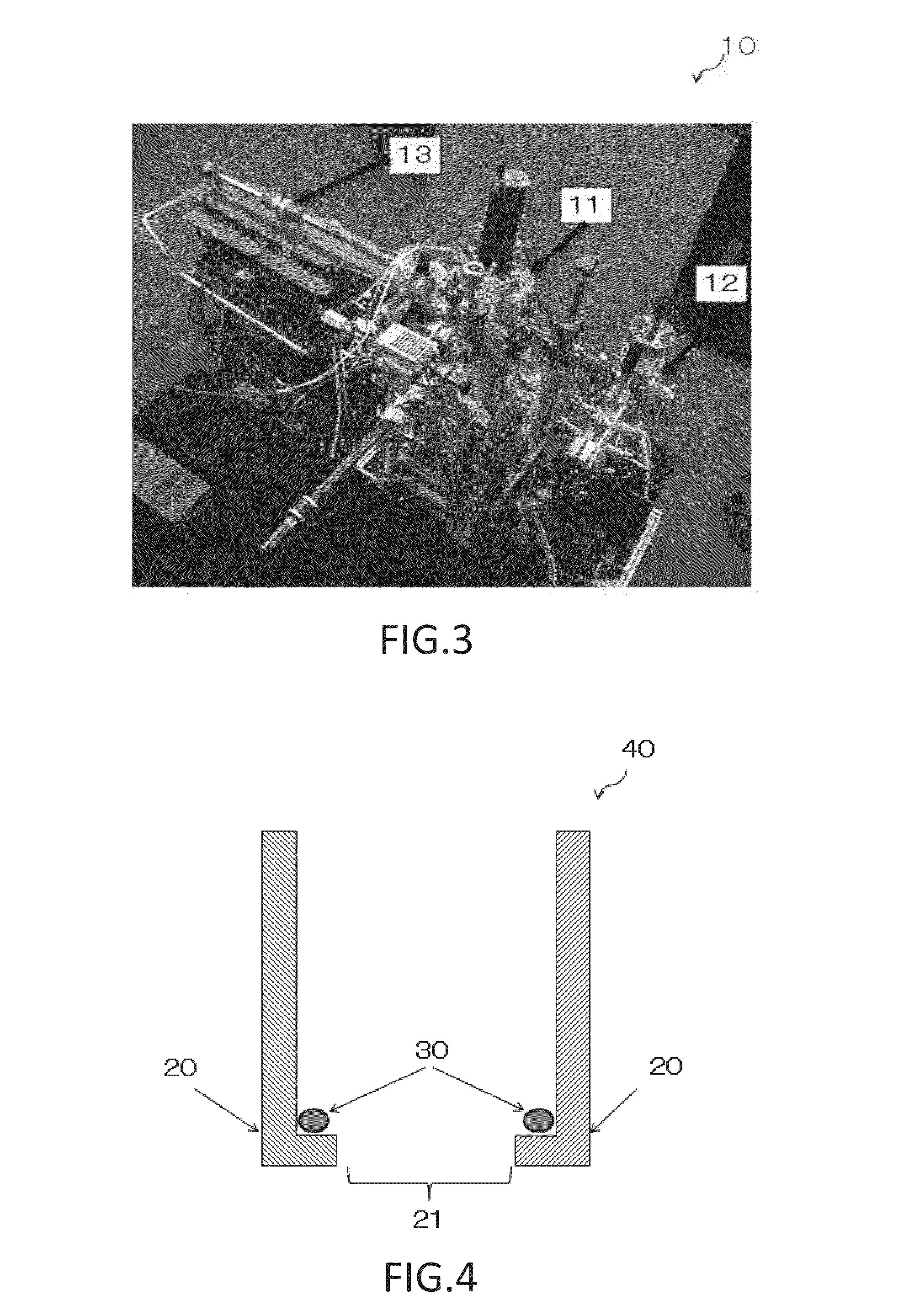
However, in cases in which the EA surface treatment chamber and the electron gun chamber are furnished separately, firstly, two chambers brought to an ultrahigh vacuum state are needed; and further, the transport means 13 is needed to transport the photocathode treated in the EA surface treatment chamber into the electron gun chamber while continuing to maintain the ultrahigh vacuum state, leading to the problem that the electron gun device becomes extremely large.
Moreover, because it is necessary for the EA surface-treated photocathode to be moved from the EA surface treatment chamber to the electron gun chamber and installed therein while maintaining an ultrahigh vacuum, and also to be moved from the EA surface treatment chamber to the electron gun chamber and installed therein during EA surface re-treatment of the photocathode, the device must be designed precisely, and proper manipulation of the photocathode is necessary to avoid dropping it during transport, leading to the problem of complicated device management.[Non-Patent Document 1] MRS-J NEWS, Vol. 20, No. 2, May 2008

Method used


Image

  • Activation chamber and kit used in treatment device for lowering electron affinity, treatment device that contains said kit and is used to lower electronic affinity, photocathode electron-beam source, electron gun containing photocathode electron-beam source, free-electron laser accelerator, transmission electron microscope, scanning electron microscope, electron-beam holography microscope, electron-beam lithography device, electron-beam diffraction device, and electron-beam scanning device
  • Activation chamber and kit used in treatment device for lowering electron affinity, treatment device that contains said kit and is used to lower electronic affinity, photocathode electron-beam source, electron gun containing photocathode electron-beam source, free-electron laser accelerator, transmission electron microscope, scanning electron microscope, electron-beam holography microscope, electron-beam lithography device, electron-beam diffraction device, and electron-beam scanning device
  • Activation chamber and kit used in treatment device for lowering electron affinity, treatment device that contains said kit and is used to lower electronic affinity, photocathode electron-beam source, electron gun containing photocathode electron-beam source, free-electron laser accelerator, transmission electron microscope, scanning electron microscope, electron-beam holography microscope, electron-beam lithography device, electron-beam diffraction device, and electron-beam scanning device

Examples


example 1

Fabrication of Activation Chamber

[0088]Using molybdenum as the material, an activation chamber was formed by cutting and surface polishing. The bottom surface was circular with a diameter of 68 mm, and the hole diameter was 11 mm.

[0089](Fabrication of Kit)

example 2

Fabrication of Fastening Member Having Surface Treatment Materials Fitted to Distal End

[0090]To the distal end of a ceramic fastening member 36 fabricated by cutting and hardening were fitted four surface treatment materials 30 (made by SAE Getters) of Cs2CrO4 having heating wiring inserted through the center. Silver electrical wire for energizing and heating the heating wiring was wired inside the fastening member 36. FIG. 20 is a photo showing the outward appearance of a fastening member having the fabricated surface treatment materials fitted to the distal end.

[0091](Fabrication of Photocathode Rod, and Photocathode Holder with Photocathode Material Attached)

[0092]The photocathode rod 50 was fabricated from titanium. The photocathode holder 51 was fabricated from molybdenum, and was approximately 34 mm in diameter. Next, a sapphire substrate on which a GaN semiconductor was grown was attached to the molybdenum with melted indium, to produce the photocathode holder 51 with the pho...

example 3

[0095]The kit fabricated in Example 2 was placed inside a vacuum chamber (Spherical Chamber made by Kimball Physics Inc.). Using a ribbon heater as heating means, the interior of the vacuum chamber was evacuated to 10−9 Pa by a vacuum pump (an ion pump made by ULVAC, or a non-evaporable getter pump made by SAES Getter), and evacuated to an ultrahigh vacuum state. The photocathode material was heated for 1 hour at approximately 550° C., removing surface impurities such as oxides and carbides. Next, a fastening member with the surface treatment material fabricated in Example 2 fitted to the distal end was energized and heated to approximately 600° C., vaporizing the surface treatment material, and Cs was vapor-deposited onto the surface of the photocathode material for 10 minutes, followed by spraying oxygen (99.999%) onto the photocathode material for 2 minutes. Spraying of the surface treatment material and the oxygen was carried out five times to carry out EA surface treatment of t...


PUM


Abstract

This invention provides a treatment device for lowering electron affinity, said treatment device being capable of performing an EA surface treatment on a photocathode material or an EA surface retreatment on a photocathode, and an electron-beam device provided with said treatment device. An activation chamber (20) used in a treatment device for lowering electron affinity by vaporizing a surface-treatment material (30) and using the vaporized surface-treatment material (30) to perform an electron-affinity lowering treatment on a photocathode material (52) or an electron-affinity lowering retreatment on a photocathode (52), said activation chamber (20) being characterized by containing holes through which electrons can pass.

Description

BACKGROUND OF THE INVENTION[0001]1. Field of the Invention[0002]The present invention relates to an activation chamber and a kit used in a treatment device for lowering electron affinity; a treatment device containing the kit and used to lower electron affinity; a photocathode electron-beam source; an electron gun containing a photocathode electron-beam source; a free-electron laser accelerator containing a photocathode electron-beam source; a transmission electron microscope containing a photocathode electron-beam source; a scanning electron microscope containing a photocathode electron-beam source; an electron-beam holography microscope containing a photocathode electron-beam source; an electron-beam lithography device containing a photocathode electron-beam source; an electron-beam diffraction device containing a photocathode electron-beam source; and an electron-beam scanning device containing a photocathode electron-beam source; and relates in particular to an activation chambe...

Claims


Application Information

Patent Timeline
Patent Type & Authority Applications(United States)
IPC IPC(8): H01J1/34H01J37/06
CPCH01J1/34H01J37/06H01J2237/2602H01J2237/31715H01J2237/06333H01J37/073
Inventor NISHITANI, TOMOHIRO
Owner PHOTO ELECTRON SOUL INC
Learn More