
Pre-clean of silicon germanium for pre-metal contact at source and drain and pre-high k at channel

a technology of silicon germanium and pre-metal contact, applied in the field of pre-cleaning, can solve the problems of difficult removal during the cleaning of the substrate, negatively affecting the quality of the epitaxial layer, and susceptible surfaces of monocrystalline silicon and epitaxial silicon layers

Active Publication Date: 2016-03-17
APPLIED MATERIALS INC
View PDF1 Cites 101 Cited by
  • Summary
  • Abstract
  • Description
  • Claims
  • Application Information

AI Technical Summary

Benefits of technology

The present invention relates to methods for removing contaminants and native oxides from substrate surfaces, particularly silicon germanium substrates with a high germanium concentration. The methods involve exposing the substrate surface to hydrogen radical species, followed by a plasma formed from a fluorine-containing precursor and a hydrogen-containing precursor, and then a second plasma with hydrogen radical species. Additionally, annealing the substrate and forming an epitaxial layer on the surface can be carried out in a single processing system without breaking vacuum. The methods provide a way to effectively remove surface impurities and improve the quality of epitaxial layers for various semiconductor devices.

Problems solved by technology

Surfaces of the monocrystalline silicon and the epitaxial silicon layer are susceptible to contamination when exposed to ambient conditions at a typical substrate fabrication facility.
The presence of native oxides of germanium, silicon-germanium alloy, or carbon residues on the germanium-doped silicon surface not only negatively affects the quality of an epitaxial layer subsequently formed on the germanium-doped silicon surface, but is also difficult to remove during cleaning of the substrate.

Method used


Image

  • Pre-clean of silicon germanium for pre-metal contact at source and drain and pre-high k at channel
  • Pre-clean of silicon germanium for pre-metal contact at source and drain and pre-high k at channel
  • Pre-clean of silicon germanium for pre-metal contact at source and drain and pre-high k at channel

Examples


Embodiment Construction

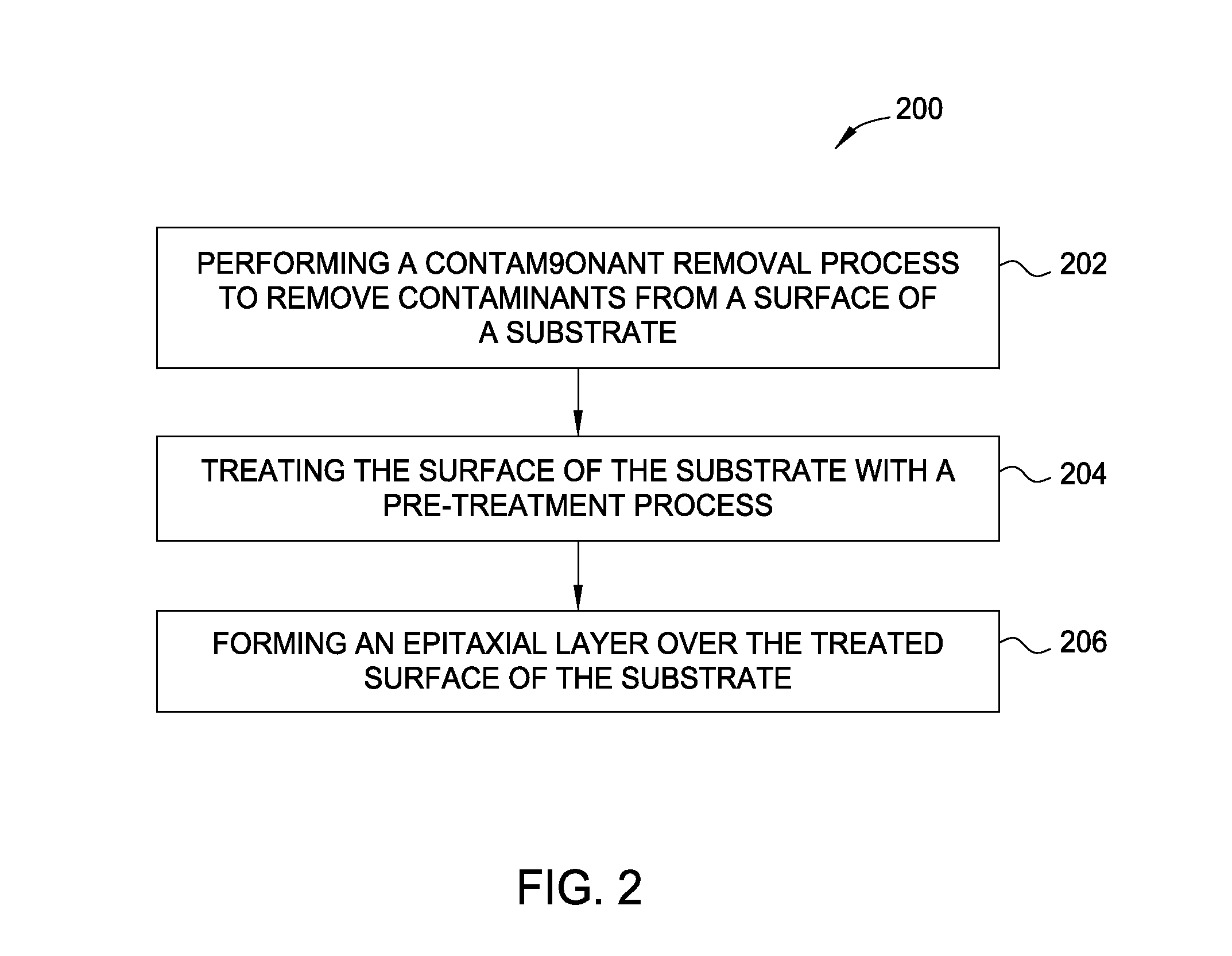
[0018]Implementations of the present disclosure generally relate to methods for removing contaminants and native oxides from substrate surfaces. The methods generally include removing contaminants disposed on the substrate surface using hydrogen radicals, and then cleaning the substrate surface by use of a remote plasma assisted dry etch process.

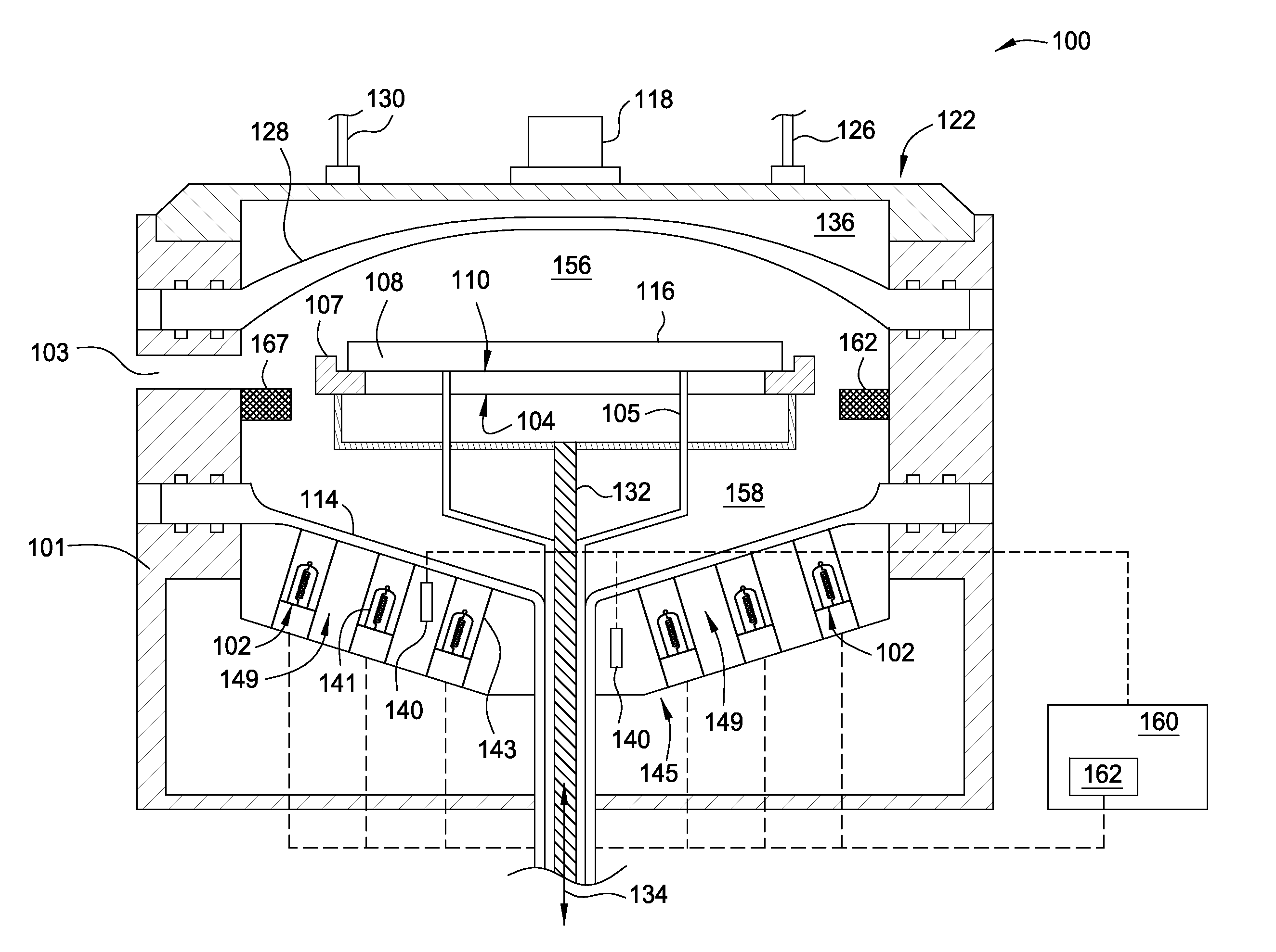
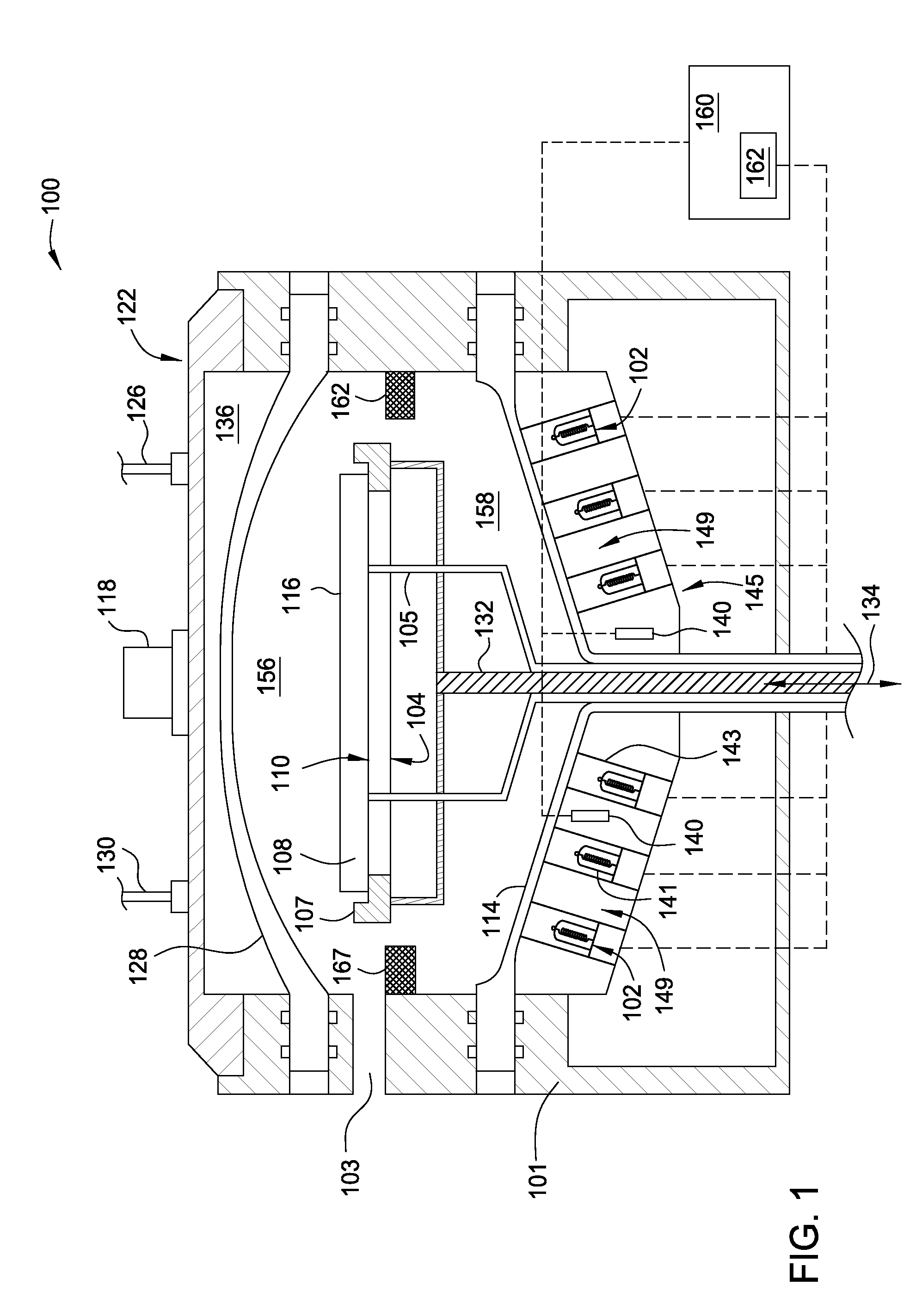
[0019]FIG. 1 is a schematic cross-sectional view of a processing chamber 100 that may be used to perform certain processes according to implementations of the present disclosure. The processing chamber 100 may be used to process one or more substrates, including the deposition of a material on an upper surface of a substrate 108. The processing chamber 100 generally includes an array of radiant heating lamps 102 for heating, among other components, a back side 104 of a substrate support 107 disposed within the processing chamber 100. The substrate support 107 may be a ring-like substrate support as shown, which supports the substrate from th...


PUM

PropertyMeasurementUnit
thicknessaaaaaaaaaa
thicknessaaaaaaaaaa
thicknessaaaaaaaaaa

Abstract

The present disclosure generally relates to methods for removing contaminants and native oxides from substrate surfaces. The method includes exposing a surface of the substrate to first hydrogen radical species, wherein the substrate is silicon germanium having a concentration of germanium above about 30%, then exposing the surface of the substrate to a plasma formed from a fluorine-containing precursor and a hydrogen-containing precursor, and then exposing the surface of the substrate to second hydrogen radical species.

Description

CROSS-REFERENCE TO RELATED APPLICATIONS[0001]This application claims benefit of U.S. provisional patent application Ser. No. 62 / 050,695, filed Sep. 15, 2014, which is herein incorporated by reference.BACKGROUND[0002]1. Field[0003]Implementations of the present disclosure generally relate to methods and apparatuses for removing contaminants and oxides from a substrate surface.[0004]2. Description of the Related Art[0005]Integrated circuits are formed in and on silicon and other semiconductor substrates. In the case of single crystal silicon, substrates are made by growing an ingot from a bath of molten silicon, and then sawing the solidified ingot into multiple wafers. An epitaxial silicon layer may then be formed on the monocrystalline silicon wafer to form a defect free silicon layer that may be doped or undoped. Semiconductor devices, such as transistors, are manufactured from the epitaxial silicon layer. The electrical properties of the formed epitaxial silicon layer will general...

Claims


Application Information

Patent Timeline
Patent Type & Authority Applications(United States)
IPC IPC(8): H01L21/02H01L21/324H01L29/161
CPCH01L21/02661H01L21/324H01L21/02068H01L21/02532H01L21/02639H01L29/161C23C16/0245C23C16/4405C23C16/481H01L21/02046H01L21/02049H01L21/02057H01L21/02381H01L21/67115H01L21/67184H01L21/67207
Inventor ZHENG, BOGELATOS, AVGERINOS V.VYAS, ANSHULHUNG, RAYMOND HOIMAN
Owner APPLIED MATERIALS INC
Learn More