Image reading apparatus and method of controlling the same, and storage medium
a reading apparatus and reading method technology, applied in the direction of color television details, television system details, television systems, etc., can solve the problems of inability to apply a technique, unstable voltage output in the reset noise, and difficult stable sampling of reset noise including variation of the cdd sensor, etc., to achieve the effect of reliably detecting an abnormal connection of the reading sensor
- Summary
- Abstract
- Description
- Claims
- Application Information
AI Technical Summary
Benefits of technology
Problems solved by technology
Method used
Image
Examples
first embodiment
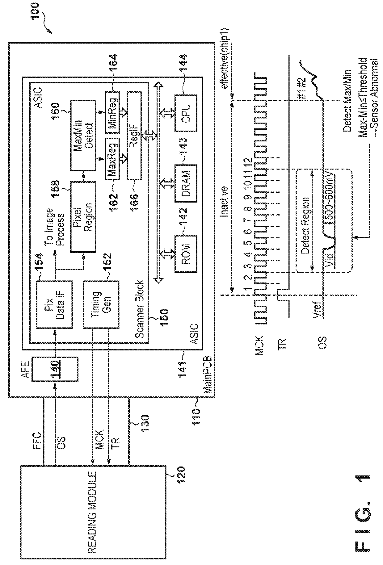
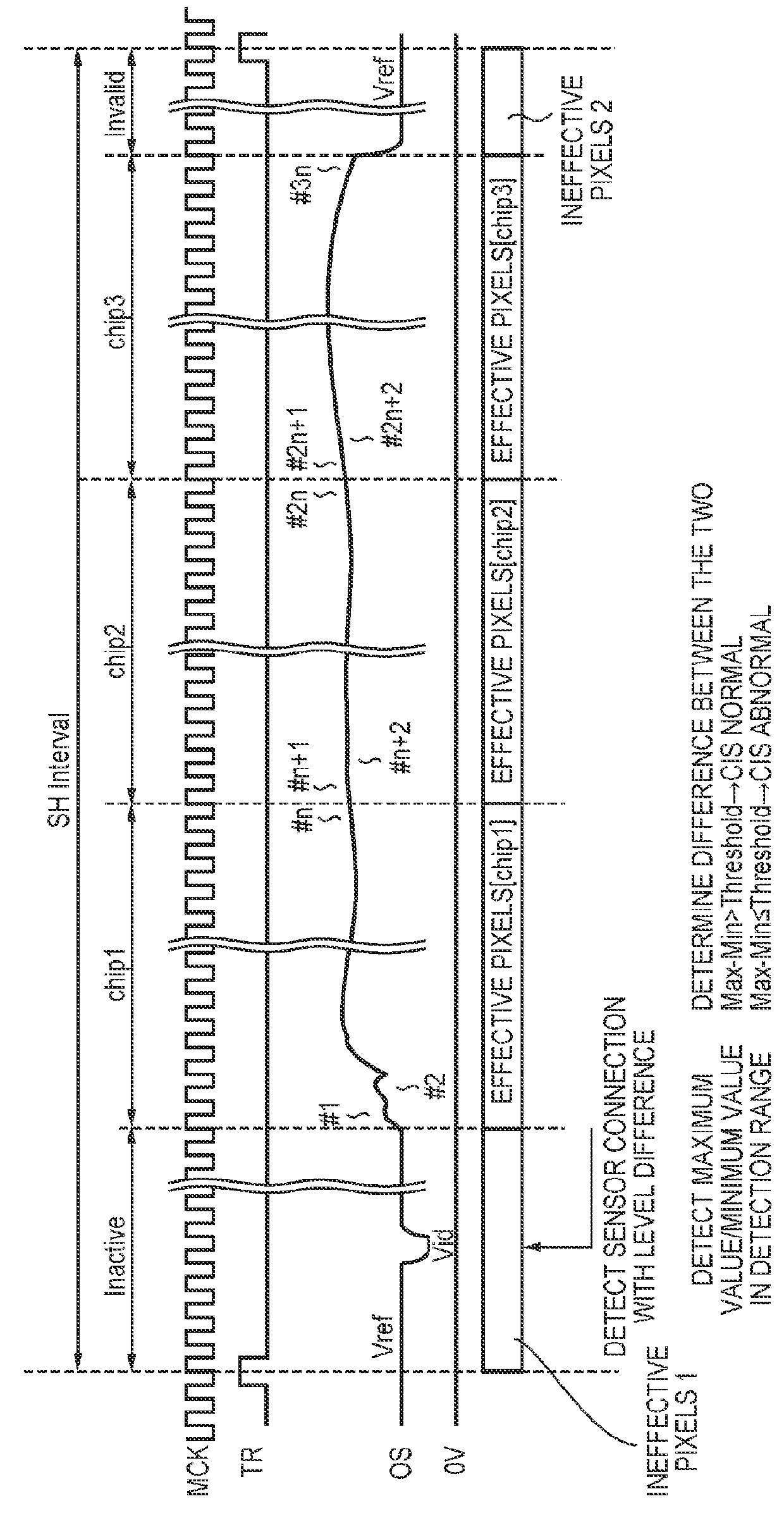
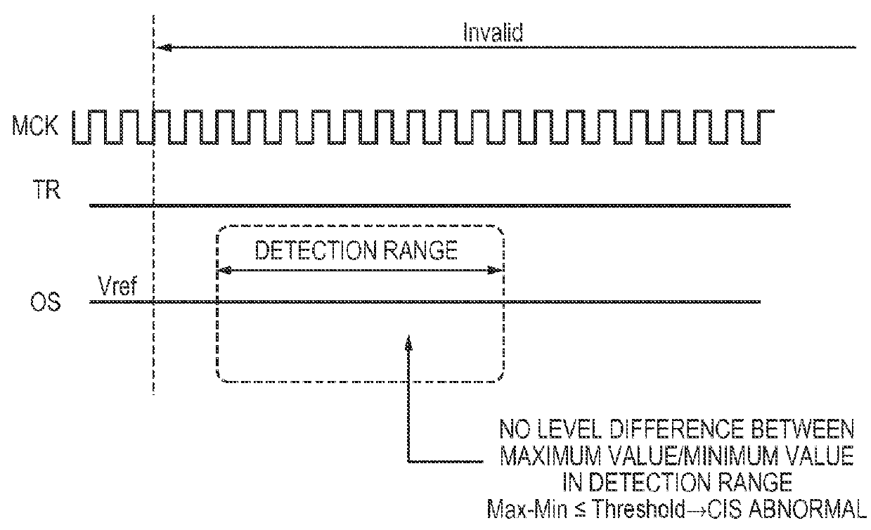
[0028]FIG. 1 is a diagram showing an overall configuration of an image reading apparatus according to a first embodiment of the present invention. In FIG. 1, an image reading apparatus 100 is configured such that a main circuit board 110 of an image reading apparatus main body and a reading module 120 are connected via an FFC (Flexible Flat Cable) 130. An AFE (Analog Front End) 140 that performs A / D conversion on analog image signals from the reading module 120 and an ASIC (Application Specific Integration Circuit) 141 that performs overall control of the reading apparatus are included on the main circuit board 110. A scanner block 150 is included in the ASIC 141. A TG (Timing Generator) 152 that generates signals that drive a reading sensor inside the reading module 120 is arranged in the scanner block 150. Also, other members arranged in the scanner block include a Pix Data IF (Image Interface) 154 that receives signals from the AFE 140 and converts them into pixel values, a Pixel...
second embodiment
[0064]FIG. 10A and FIG. 10B show a sensor output timing chart of the reading module of a second embodiment. A major difference with the first embodiment is that the operations of inserting and not inserting an identification signal are switched by changing the pulse width of the line synchronization signal TR.
[0065]In the case in which the identification signal is to be inserted, the pulse width of the TR set wide, and in the case in which the identification signal is not to be inserted, the pulse width of the TR is set narrow. Accordingly, the switching of the operation mode is performed within the sensor chip. In an actual configuration, the pulse width of the line synchronization signal is detected in the timing signal generation circuit 702 shown in FIG. 7, which shows the internal configuration of the sensor chip, and there is a switch between whether or not to activate the timing Pid signal for insertion of the identification signal.
[0066]According to the present embodiment, t...
third embodiment
[0067]FIG. 11A and FIG. 11B show timing charts of a third embodiment. A difference with the first embodiment is the pixel position of the output of the connection identification signal. In the first embodiment, the identification signal is inserted immediately after the line synchronization signal, but in the third embodiment, the identification signal is inserted after pixel output corresponding to all of the pixels has been output.
[0068]FIG. 11A is a timing chart in the case in which connection detection is performed, and FIG. 11B is a timing chart in the case in which an image is scanned. When connection detection is to be performed, the number of pixels in one line from the pixel position of the identification signal is set high, and when an image is to be scanned, the number of pixels in one line is set smaller than the pixel position of the identification signal, and thus it is possible to insert the identification signal only when connection detection is to be performed.
[0069...
PUM
 Abstract
Description
Claims
Application Information
 - R&D
- Intellectual Property
- Life Sciences
- Materials
- Tech Scout
- Unparalleled Data Quality
- Higher Quality Content
- 60% Fewer Hallucinations
Browse by: Latest US Patents, China's latest patents, Technical Efficacy Thesaurus, Application Domain, Technology Topic, Popular Technical Reports.
© 2025 PatSnap. All rights reserved.Legal|Privacy policy|Modern Slavery Act Transparency Statement|Sitemap|About US| Contact US: help@patsnap.com


