Semiconductor Device, Display Module, and Electronic Appliance
a technology of semiconductor devices and display modules, applied in the direction of static indicating devices, solid-state devices, instruments, etc., can solve the problems of difficult to reduce a layout area, difficult to reduce the /l of transistors, and long etc., to achieve the effect of reducing the time required for changing the potential of nodes in circuits, reducing the drain current of transistors, and improving the effect of circuit stability
- Summary
- Abstract
- Description
- Claims
- Application Information
AI Technical Summary
Benefits of technology
Problems solved by technology
Method used
Image

Examples
embodiment 1
[0065]In this embodiment, a semiconductor device of one embodiment of the present invention will be described.
[0066]A structure of a semiconductor device of one embodiment of the present invention will be described with reference to FIG. 1. Note that one embodiment of the present invention is not limited to the structure described below.
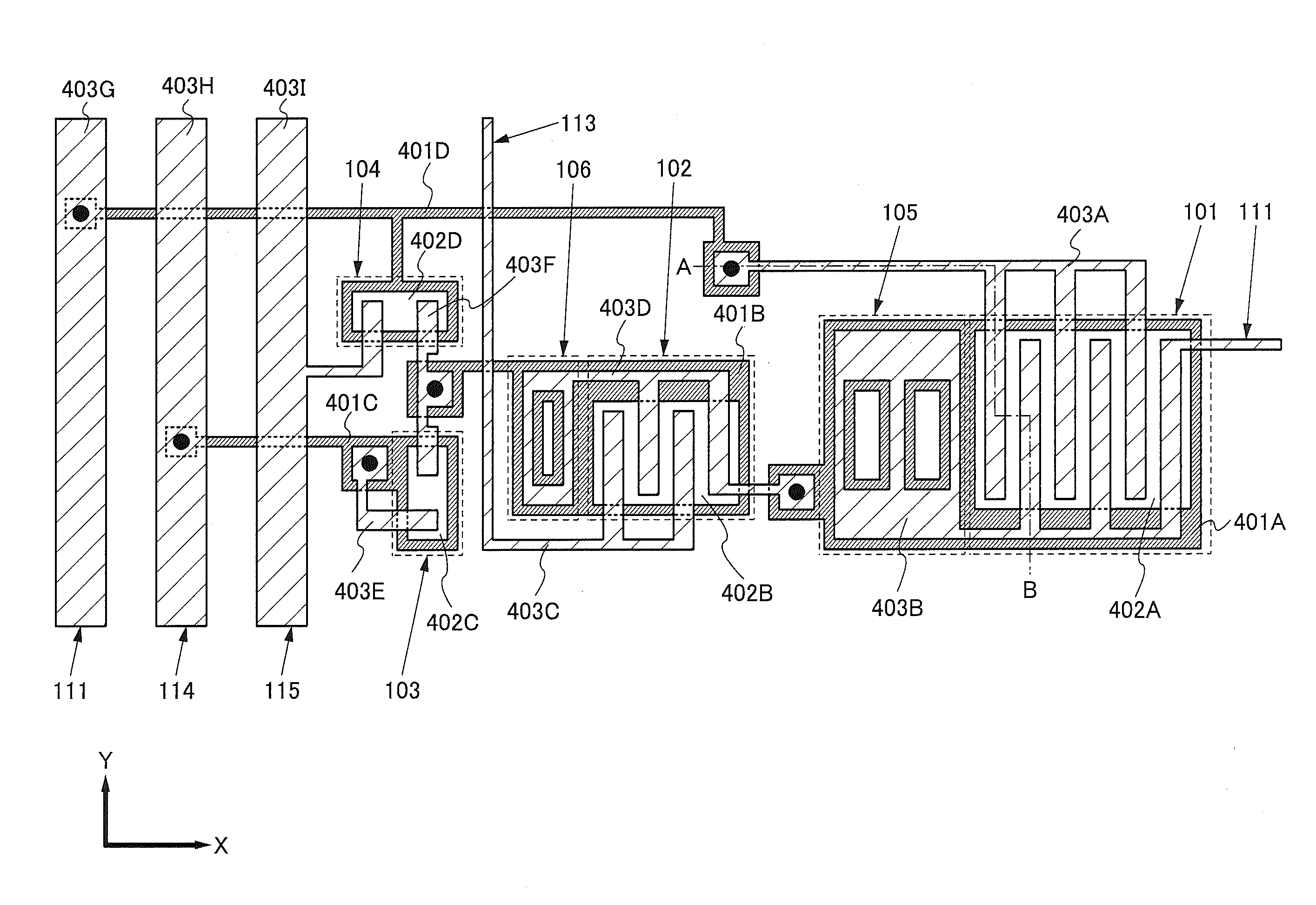
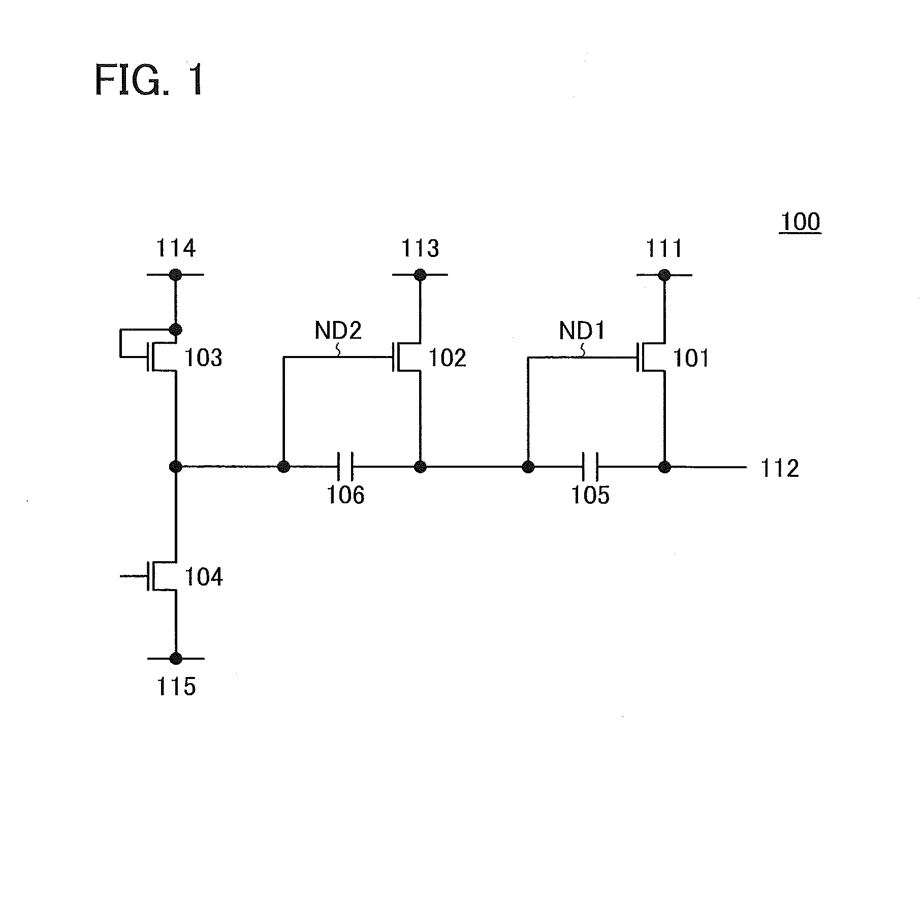
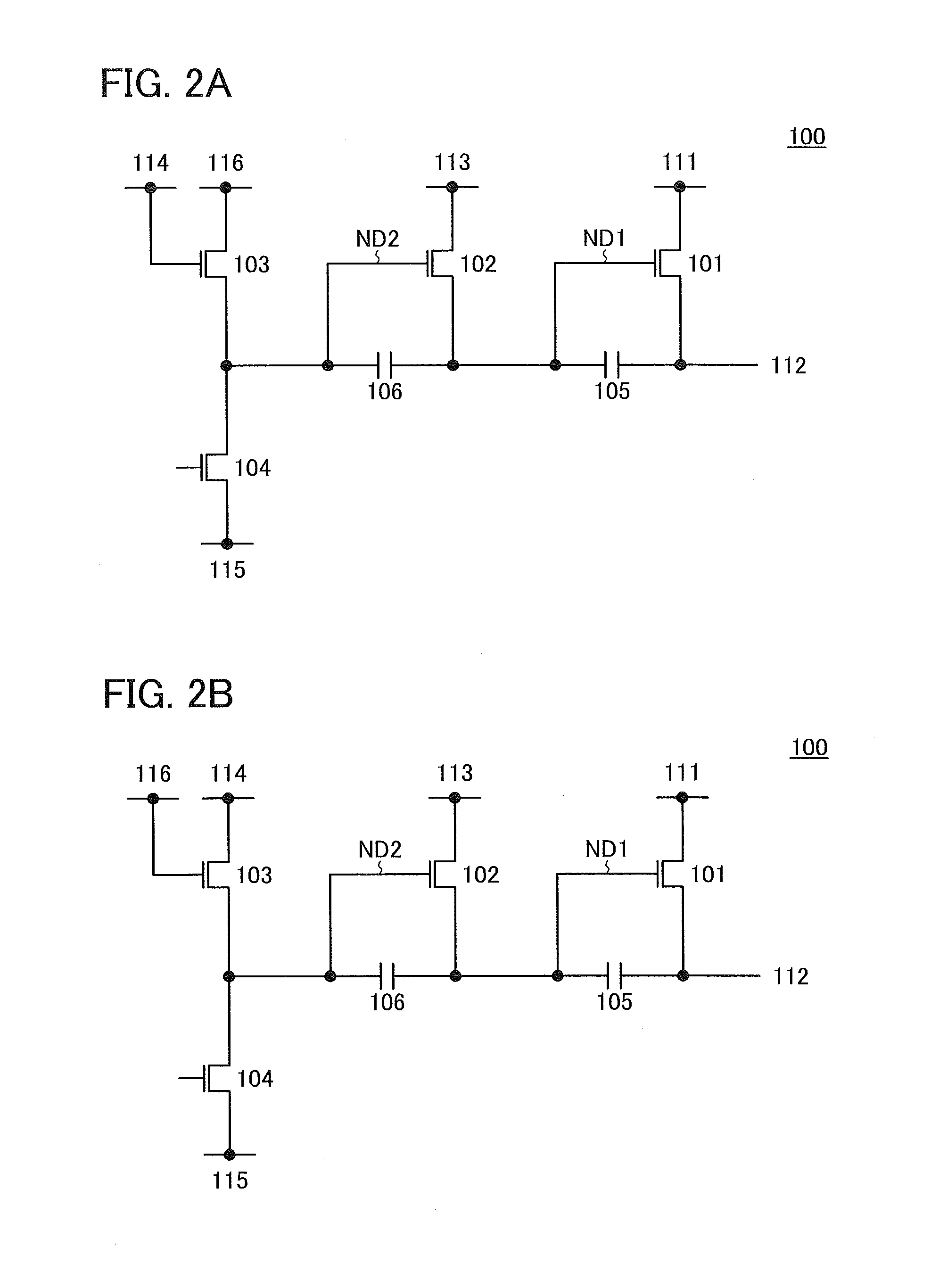
[0067]A semiconductor device illustrated in FIG. 1 includes a circuit 100. The circuit 100 has a function of controlling the potential of a wiring 112 based on the potentials of a wiring 111, a wiring 113, a wiring 114, and a wiring 115. The circuit 100 outputs a signal based on the potentials of the wiring 111, the wiring 113, the wiring 114, and the wiring 115 to the wiring 112. The potential of the wiring 112 is controlled by the signal. As described above, the circuit 100 serves as a logic circuit or a sequential circuit.
[0068]The circuit 100 includes a transistor 101, a transistor 102, a transistor 103, a transistor 104, a capacitor 105, and a c...
embodiment 2
[0187]In this embodiment, a semiconductor device of one embodiment of the present invention is described.
[0188]A structure of a semiconductor device of one embodiment of the present invention is described with reference to FIG. 15. Note that one embodiment of the present invention is not limited to the structure described below.
[0189]A semiconductor device illustrated in FIG. 15 includes a circuit 200. The circuit 200 has a function of controlling potentials of N (N is a natural number of 3 or more) wirings 211 (also referred to as wirings 211[1] to [N]) based on potentials of a wirings 212, 213, 214, and 215. The circuit 200 outputs signals based on the potentials of the wirings 212, 213, 214, and 215 to the corresponding wirings 211[1] to [N]. The potentials of the wirings 211 [1] to [N] are controlled with the signals.
[0190]Specifically, based on the potentials of the wirings 212, 213, 214, and 215, the circuit 200 has a function of sequentially making the potentials of the wirin...
embodiment 3
[0200]In this embodiment, a display device of one embodiment of the present invention is described.
[0201]A structure of a display device of one embodiment of the present invention is described with reference to FIG. 19. Note that one embodiment of the present invention is not limited to the structure described below.
[0202]A display device illustrated in FIG. 19 includes a pixel portion 301, a scan line driver circuit 302, and a signal line driver circuit 303.
[0203]In the pixel portion 301, N scan lines GL (also referred to as scan lines GL [1] to [N]) and M (M is a natural number of two or more) signal lines SL (also referred to as signal lines SL [1] to [M]) are provided so as to intersect with each other. A pixel 310 is provided at each intersection.
[0204]The pixel 310 includes at least a display element and a transistor. Examples of a display element include a light-emitting element and a liquid crystal element. An example of a light-emitting element includes an EL element.
[0205]...
PUM
 Abstract
Description
Claims
Application Information
 - R&D
- Intellectual Property
- Life Sciences
- Materials
- Tech Scout
- Unparalleled Data Quality
- Higher Quality Content
- 60% Fewer Hallucinations
Browse by: Latest US Patents, China's latest patents, Technical Efficacy Thesaurus, Application Domain, Technology Topic, Popular Technical Reports.
© 2025 PatSnap. All rights reserved.Legal|Privacy policy|Modern Slavery Act Transparency Statement|Sitemap|About US| Contact US: help@patsnap.com