Semiconductor light-emitting element and method for manufacturing the same

a technology of semiconductor light-emitting elements and manufacturing methods, which is applied in the direction of semiconductor lasers, semiconductor devices, electrical apparatus, etc., can solve the problems of parasitic capacitance in these already small devices becoming critical in the speed of operation, and achieve the effects of reducing parasitic capacitance, low dielectric constant, and improving high frequency performan

Active Publication Date: 2015-12-31
CLOUD LIGHT TECH LTD
View PDF5 Cites 7 Cited by
  • Summary
  • Abstract
  • Description
  • Claims
  • Application Information

AI Technical Summary

Benefits of technology

[0007]One objective of the present invention is to provide a semiconductor light-emitting element, which has low dielectric constant and reduced electri...

Problems solved by technology

As the device speeds increase, electrical parasitics limit the performance of high-speed, the device impedance and pad capacitances are increasingly becomes design fa...

Method used


Image

  • Semiconductor light-emitting element and method for manufacturing the same
  • Semiconductor light-emitting element and method for manufacturing the same
  • Semiconductor light-emitting element and method for manufacturing the same

Examples


Embodiment Construction

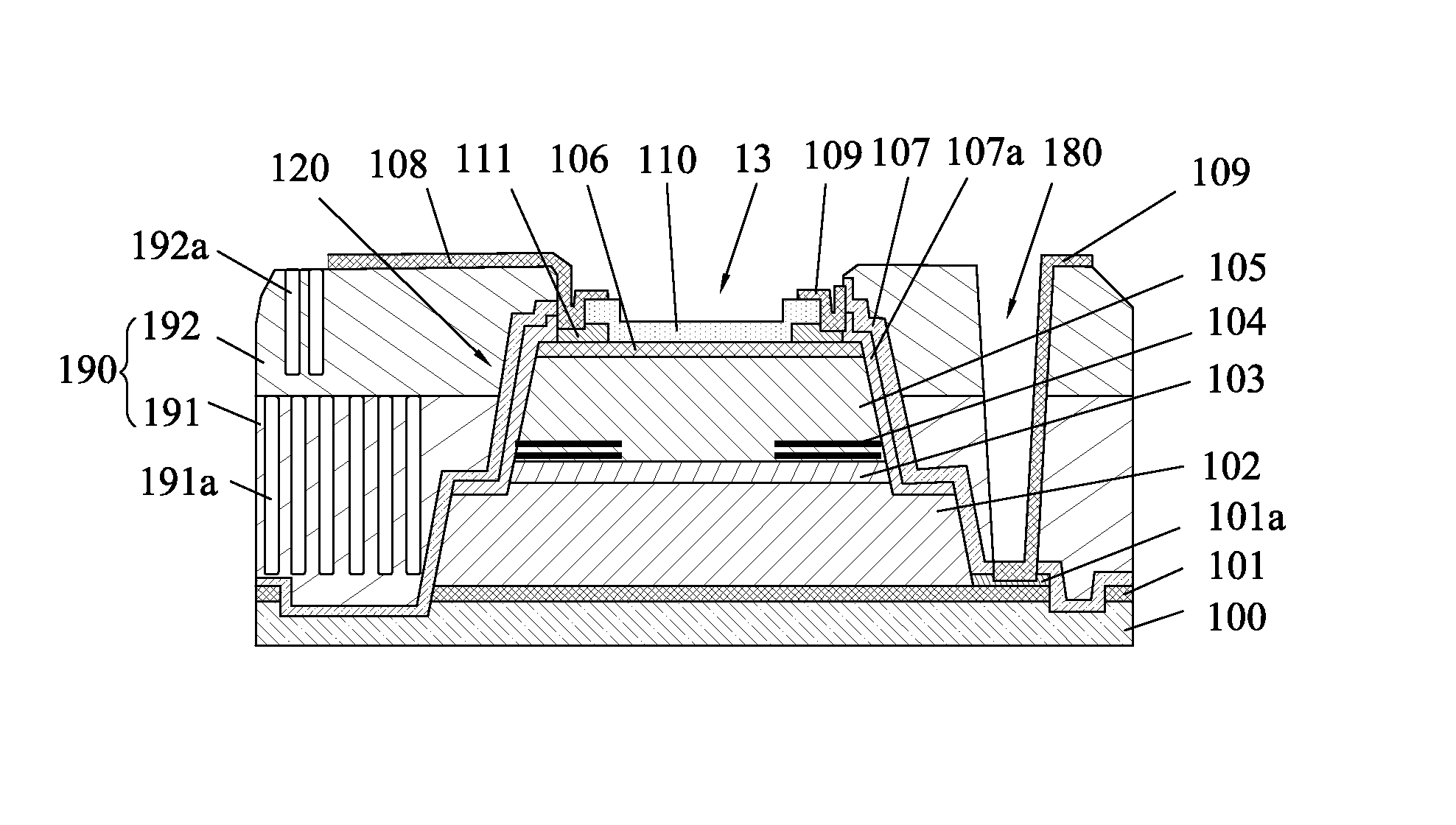
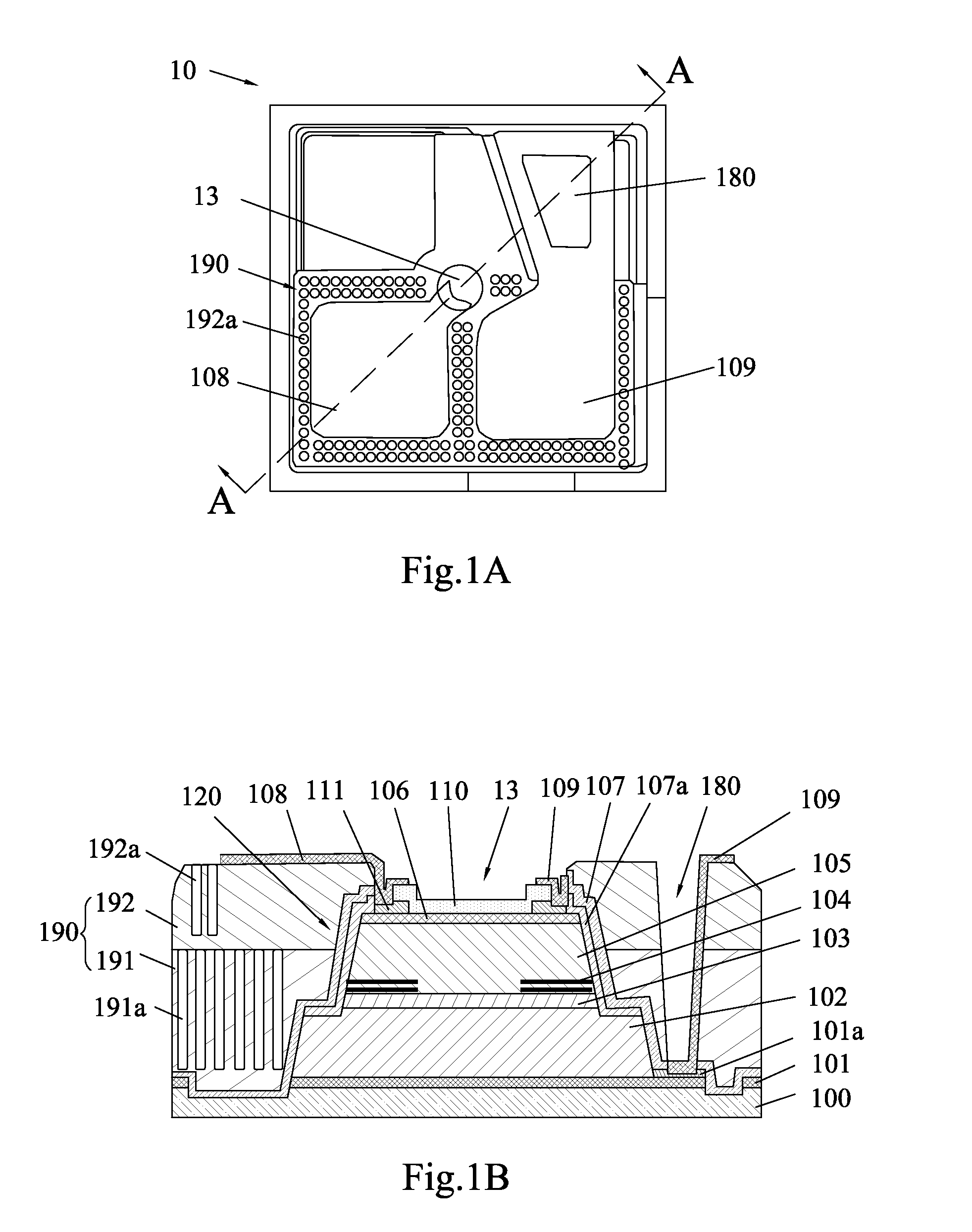
[0048]Various preferred embodiments of the invention will now be described with reference to the figures, wherein like reference numerals designate similar parts throughout the various views. As indicated above, the invention is directed to a semiconductor light-emitting element and a manufacturing method thereof, which has low dielectric constant and reduced electrical parasitics especially parasitic capacitances, thereby improving high frequency performance and improving modulation speed of light-emitting device finally.

[0049]Referring to FIGS. 1A and 1B, a semiconductor lighting-emitting element 10 according to one embodiment of the present invention includes a substrate 100, and multilayer structure formed on the substrate 100, which includes a lower n-type contact layer 101, a lower reflecting mirror film 102 made of an n-type semiconductor multilayer film, an active layer 103, a current confinement layer 104, an upper reflecting mirror film 105 made of a p-type semiconductor m...


PUM


Abstract

A semiconductor light-emitting element includes: a double-mesa structure of semiconductor formed to have a cylindrical cross section; an insulating member formed to fill a space surrounding the double-mesa structure, with the insulating member comprising a lower insulating member and an upper insulting member covering the lower insulating member; and a first electrode formed on the upper insulating member to come into contact with part of a top surface of the double-mesa structure. The lower insulating member has multiple lower air pillars that are formed in an area aligning with the first electrode, and the upper insulating member has multiple upper air pillars that are formed around the first electrode. It has low dielectric constant and reduced electrical parasitics especially parasitic capacitances, thereby improving high frequency performance and improving modulation speed of light-emitting device finally.

Description

FIELD OF THE INVENTION[0001]The present invention relates to semiconductor light-emitting elements applicable to surface emitting semiconductor laser elements or the like, and methods for manufacturing such an element.BACKGROUND OF THE INVENTION[0002]In recent years, rapid increase of the Internet has pushed the amount of data transmission sharply, so that high-speed data communications networks have required.[0003]Surface emitting laser elements (or vertical cavity surface emitting laser elements (VCSELs)) are characterized in that laser light can be emitted in a perpendicular direction to the principal surface of a substrate formed with the element and in that the element has low threshold current and high power conversion efficiency. In addition to this, the surface emitting laser elements have various advantages that: they can emit circular light whose cross section perpendicular to the optical axis is circular; two-dimensional arrangement of them is facilitated; and on-wafer in...

Claims


Application Information

Patent Timeline
IPC IPC(8): H01L33/20H01L33/00H01L33/38H01L33/56H01L33/10H01L33/06
CPCH01L33/20H01L33/38H01L33/44H01S5/00H01L2933/0025H01S5/06226H01S5/18313H01S5/18333H01S5/18347H01S5/2213
Inventor PADULLAPARTHI, BABU DAYAL
Owner CLOUD LIGHT TECH LTD
Why Eureka
Try Eureka