Pixel circuit and driving method thereof
a pixel circuit and driving method technology, applied in the field of pixel circuits, can solve the problems of deteriorating contrast, inability to acquire original white display brightness, and inability to detect threshold voltage functions,
- Summary
- Abstract
- Description
- Claims
- Application Information
AI Technical Summary
Benefits of technology
Problems solved by technology
Method used
Image
Examples
first exemplary embodiment
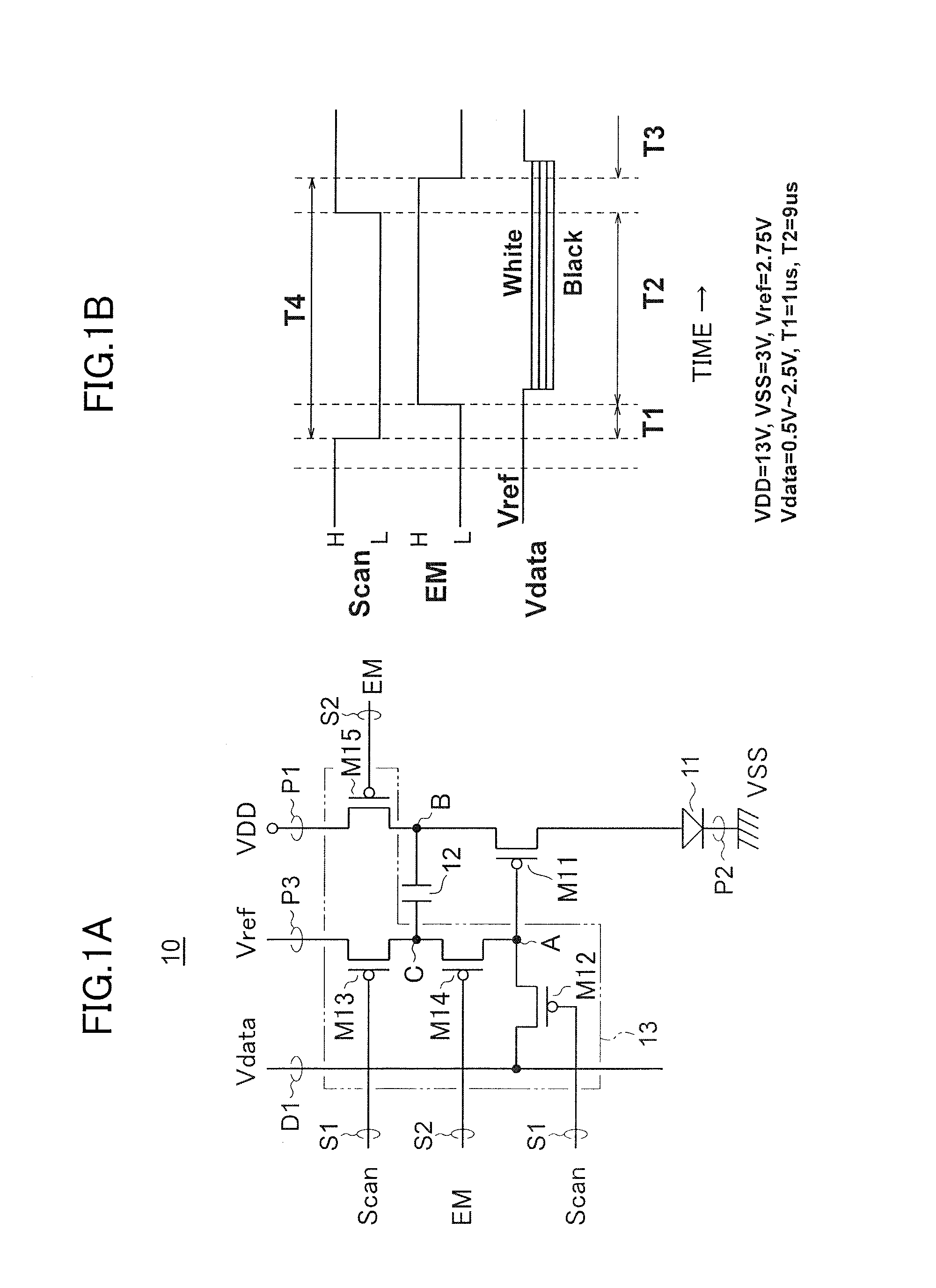
[0050]FIG. 1A is a circuit diagram showing the structure of a pixel circuit according to a first exemplary embodiment, and FIG. 1B is a timing chart showing operations of the pixel circuit of the first exemplary embodiment. Explanations will be provided hereinafter by referring to those drawings.
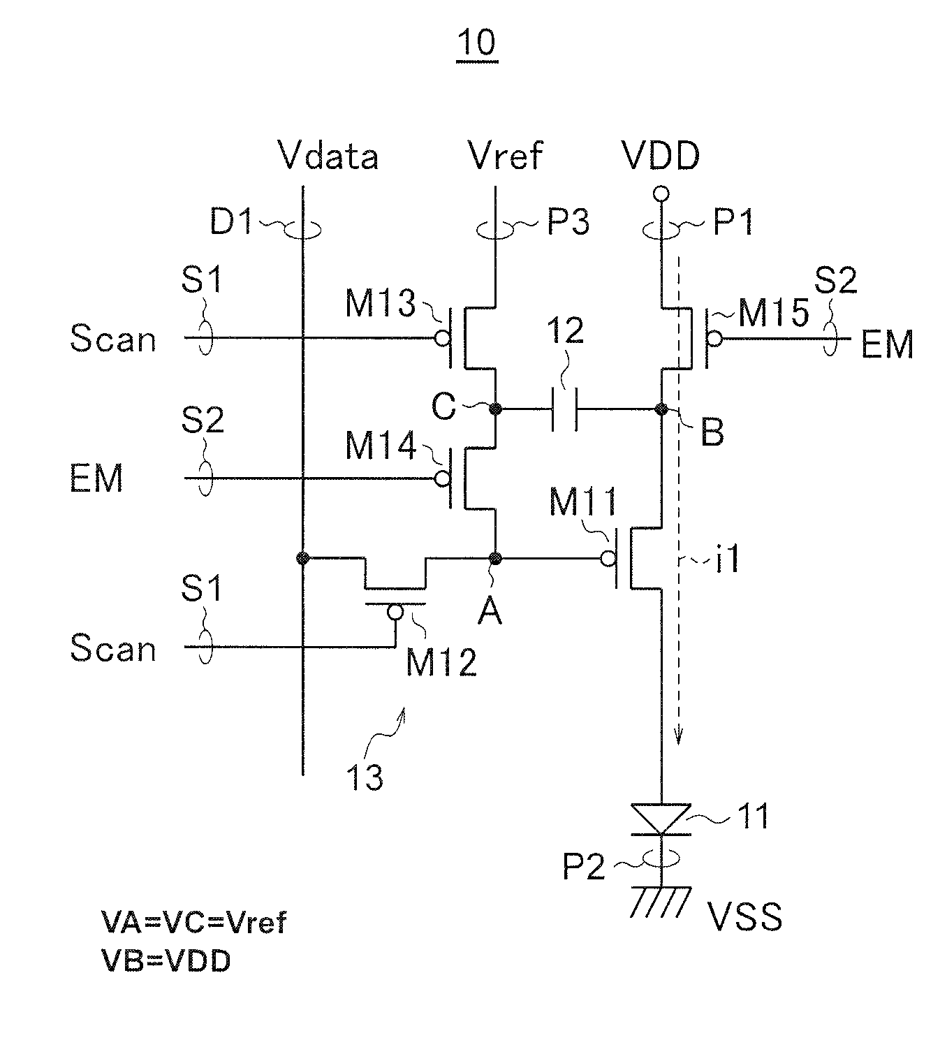
[0051]A pixel circuit 10 of the first exemplary embodiment includes: a light emitting element 11; a driving transistor (M11) which supplies an electric current to the light emitting element 11 according to an applied voltage; a capacitor part (12) which holds a voltage containing a threshold voltage Vth and a data voltage Vdata of the driving transistor (M11); and a switch part 13 which has the voltage containing the threshold voltage Vth and the data voltage Vdata held to the capacitor part (12) and applies these voltage to the driving transistor (M11). Further, the switch part 13 has a function which applies a constant voltage for preventing initialization of hysteresis characteristics to ...
second exemplary embodiment
[0095]FIG. 7A is a circuit diagram showing the structure of a pixel circuit according to a second exemplary embodiment, and FIG. 7B is a timing chart showing operations of the pixel circuit of the second exemplary embodiment. Explanations will be provided hereinafter by referring to those drawings.
[0096]A pixel circuit 20 of the second exemplary embodiment is different from that of the first exemplary embodiment in respect that a switch part 23 includes a current detour transistor (M16). The current detour transistor (M16) makes the electric current supplied from the driving transistor (M11) detour without flowing through the light emitting element 11.
[0097]Further, the switch part 13 turns on the driving transistor (M11) and the current detour transistor (M16) before having the voltage containing the threshold voltage Vth and the data voltage Vdata of the driving transistor (M11) held to the capacitor part (12).
[0098]In more detail, the switch part 23 turns on the current detour tr...
third exemplary embodiment
[0119]FIG. 11A is a circuit diagram showing the structure of a pixel circuit according to a third exemplary embodiment, and FIG. 11B is a timing chart showing operations of the pixel circuit of the third exemplary embodiment. Explanations will be provided hereinafter by referring to those drawings.
[0120]The third embodiment employs the structure in which: all the transistors of the second exemplary embodiment are replaced with the n-channel types while keeping the second terminal (cathode terminal) of the light emitting element 11 on the substrate side (VSS side); and the layout of the capacitor part (12) connected between the gate and the source as well as the accompanying transistors is changed accordingly. Therefore, the threshold voltage detecting module of the third exemplary embodiment is also a source follower type that is the same as the case of the second exemplary embodiment.
[0121]That is, the outline of a pixel circuit 30 according to the third exemplary embodiment can be...
PUM
 Abstract
Description
Claims
Application Information
 - R&D
- Intellectual Property
- Life Sciences
- Materials
- Tech Scout
- Unparalleled Data Quality
- Higher Quality Content
- 60% Fewer Hallucinations
Browse by: Latest US Patents, China's latest patents, Technical Efficacy Thesaurus, Application Domain, Technology Topic, Popular Technical Reports.
© 2025 PatSnap. All rights reserved.Legal|Privacy policy|Modern Slavery Act Transparency Statement|Sitemap|About US| Contact US: help@patsnap.com


