
OLED display panel and production process thereof

a technology production processes, applied in the field of display panels, can solve problems such as the complicated production process of oled display panels, and achieve the effects of improving the water-oxygen permeation resistance of the display panel, improving the surface flatness of the flexible base substrate, and improving the adhesion

Active Publication Date: 2015-11-26
BOE TECH GRP CO LTD +1
View PDF7 Cites 4 Cited by
  • Summary
  • Abstract
  • Description
  • Claims
  • Application Information

AI Technical Summary

Benefits of technology

The invention provides an OLED display panel and a production process that improves its surface flatness and water-oxygen resistance, and increases its light output ratio. This is achieved through the use of a special layer called a reticular light output coupling layer, which has a reticular molecular structure. This layer improves the adhesion between the display panel and the flexible base substrate, increases the water-oxygen resistance of the display panel, and acts as a transmission enhanced film to improve the light output ratio of OLED. The layer's special optical features can also be controlled to control the center wavelength of the electroluminescence spectrum and further enhance the light output ratio.

Problems solved by technology

However, it may result in the complication of the production process for the OLED panel.

Method used


Image

  • OLED display panel and production process thereof
  • OLED display panel and production process thereof
  • OLED display panel and production process thereof

Examples


Embodiment Construction

[0033]The technical solution in the invention will be clearly and completely described below, in combination with figures in the invention. Obviously, the described examples are only a part of the examples in the invention, instead of all examples. On the basis of the examples in the invention, all other examples obtained by the person skilled in the art without paying inventive labours belong to the protection scope of the invention.

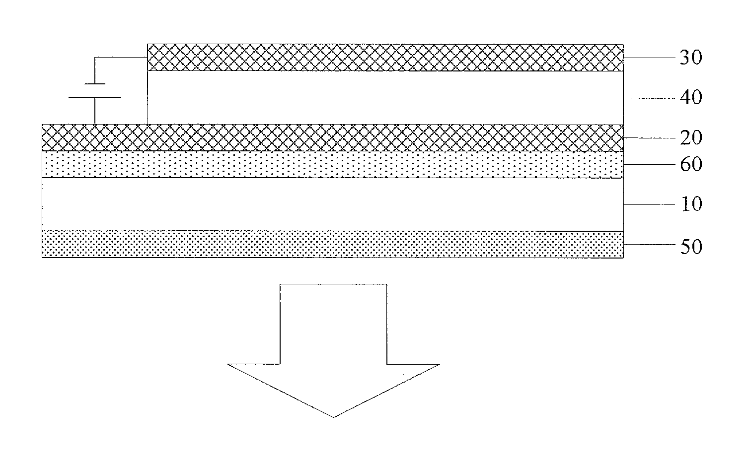
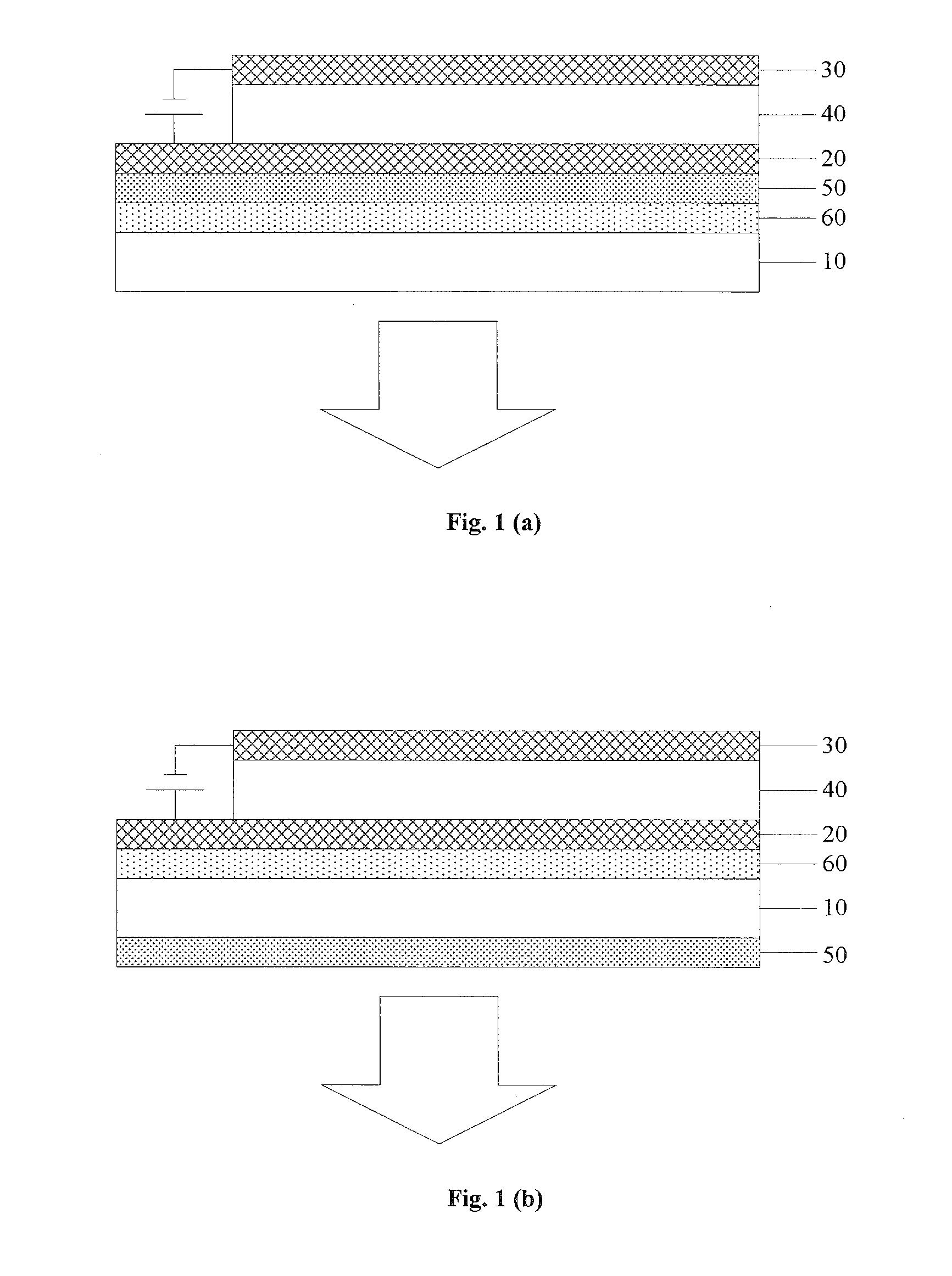
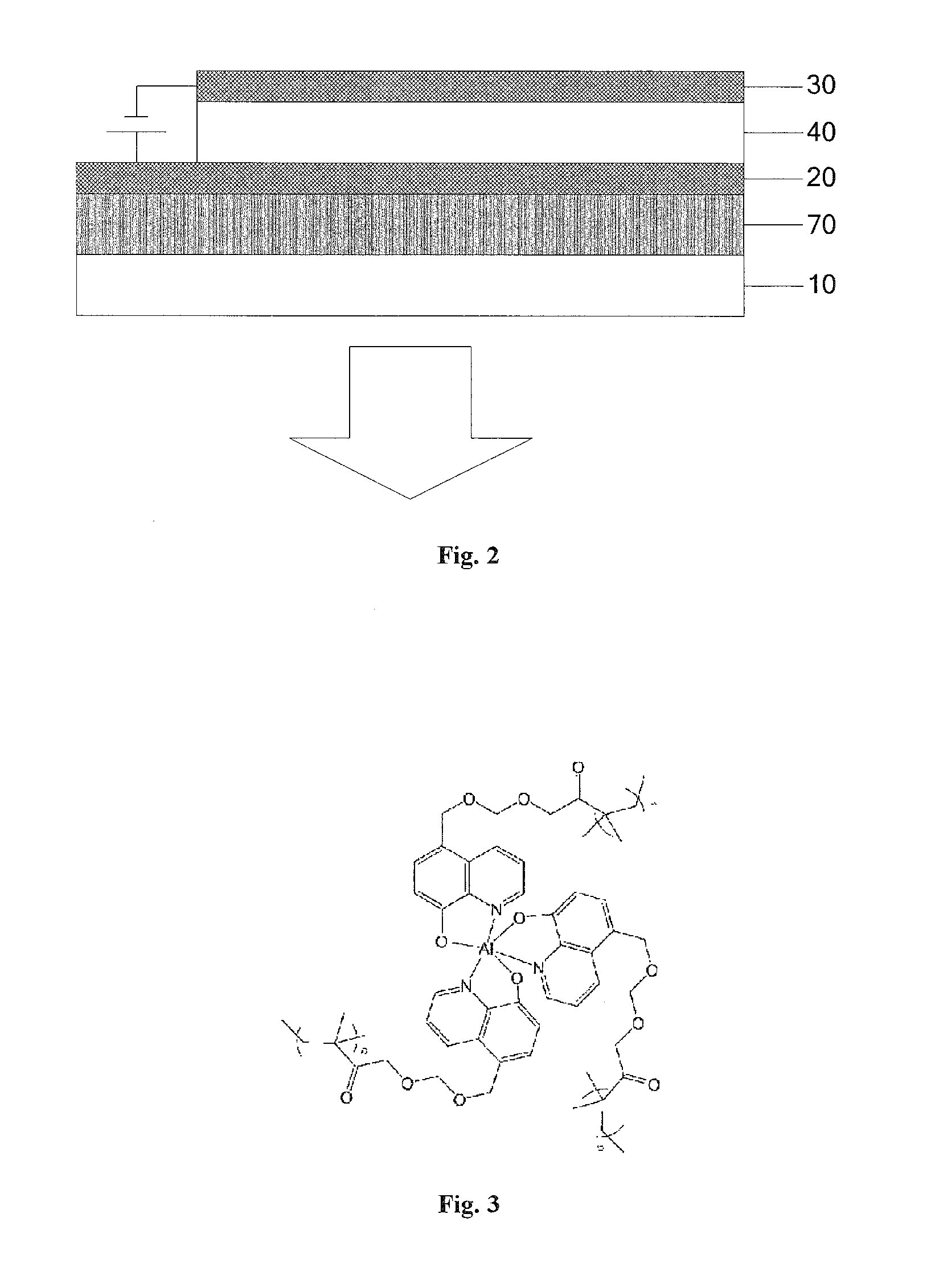
[0034]The invention provides an OLED display panel, as shown by FIG. 2, comprising an anode 20 and a cathode 30 provided on a flexible base substrate 10, and an organic material functional layer 40 provided between the anode 20 and the cathode 30; the display panel further comprises a reticular light output coupling layer 70 provided on the flexible base substrate 10 and contacting the flexible base substrate 10; wherein the anode 20, the cathode 30, and the organic material functional layer 40 are all provided on the reticular light output coupling lay...


PUM


Abstract

The invention provides an OLED display panel and the production process thereof, which relates to the technical field of display, may improve the surface flatness and the water-oxygen permeation resistance of the flexible base substrate, improve the light output ratio of the display panel, and may control the center wavelength of the electroluminescence spectrum. The display panel comprises an anode and a cathode provided on a flexible base substrate, and an organic material functional layer situated between the anode and the cathode, and it further comprises a reticular light output coupling layer provided on the flexible base substrate and contacting the flexible base substrate; the anode, the cathode, the organic material functional layer are all provided on the reticular light output coupling layer; the reticular light output coupling layer, the anode and the cathode, and the organic material functional layer compose a micro-cavity; the micro-cavity is used for controlling the center wavelength of the electroluminescence spectrum and the light output ratio. The material of the reticular light output coupling layer is a reticular high molecular material having a high refractive index and a low absorptivity in the visible light range; and it is used for the production of the flexible OLED display panel.

Description

FIELD OF THE INVENTION[0001]The invention relates to the technical field of display, especially relates to an OLED display panel and the production process thereof.BACKGROUND OF THE INVENTION[0002]Comparing with a liquid crystal display (Liquid Crystal Display, referred to as LCD), an organic electroluminescence diode device (Organic Light-Emitting Diode, referred to as OLED) has the advantages such as thin, light, broad angle of view, initiative luminescence, continuously adjustable emitting color, low cost, fast response speed, low energy cost, low driving voltage, high emitting efficiency, broad working temperature range, simple production process, and flexible display or the like, which is greatly attended by the industry and the science world.[0003]The basic structure of OLED comprises an anode 20 and a cathode 30 provided on a base substrate 10, and an organic material functional layer 40 provided between the anode 20 and the cathode 30. In order to improve the light output ra...

Claims


Application Information

Patent Timeline
Patent Type & Authority Applications(United States)
IPC IPC(8): H01L51/52H01L51/56H01L51/00H10K99/00
CPCH01L51/5237H01L51/56H01L51/5262H01L51/0097H10K59/12H10K85/60H10K59/873H10K59/879H10K59/876H10K85/324H10K77/111H10K50/84H10K50/85H10K71/00H10K50/852H10K50/858
Inventor GUO, YUANHUIWANG, HUIWANG, CHUNZHANG, YISAN
Owner BOE TECH GRP CO LTD
Learn More