Transistor element

a technology of transistor elements and transistor elements, which is applied in the direction of organic semiconductor devices, solid-state devices, thermoelectric devices, etc., can solve the problems of difficult to obtain a large current from the ofet, difficult to make the channel length several m or less, and finer display devices. , to achieve the effect of large current, excellent properties and stable operation

Active Publication Date: 2015-11-12
DAINICHISEIKA COLOR & CHEM MFG CO LTD +1
View PDF8 Cites 0 Cited by
  • Summary
  • Abstract
  • Description
  • Claims
  • Application Information

AI Technical Summary

Benefits of technology

[0031]According to the present invention, an organic transistor element (MBOT) having excellent properties described below is provided. The transistor element of the present invention is characterized in that the transistor element has a laminated structure, the laminated structure comprising: a sheet-like base electrode being arranged between an emitter electrode and a collector electrode; at least one p-type organic semiconductor layer being provided on each of the surface and back sides of the base electrode; and further a current transmission promotion layer being formed, on each of the surface and back sides of the base electrode, between the base electrode and the p-type organic semiconductor layer or layers provided on each of the surface and back sides of the base electrode. That is, in the transistor element of the present invention, at least two p-type organic semiconductor layers are arranged as described above to each of the surface and back sides of the base electrode, and further a current transmission promotion layer is provided between the base electrode and the collector electrode and between the emitter electrode and the base electrode, respectively, thereby achieving that the current modulation action which makes it possible to obtain a large current with a low voltage can stably be obtained.
[0032]The organic transistor element (MBOT) of the present invention has, as described later, high performance and is useful as an element for driving various types of displays and an organic light emitting diode, and especially useful for an element for driving an organic EL or electronic paper which is driven by the large current modulation. The transistor element which drives the above-described devices is required to have a contrast between during ON time and during OFF time, and a higher ON / OFF ratio and more suppression of dark current are required. That is, when the ON / OFF ratio is low and the dark current is large, there occurs a problem that the organic EL device emits light even during OFF time or the like. On the other hand, the transistor element of the present invention has a high ON / OFF ratio, is excellent in large current modulation property and frequency property in a low frequency region, and thereby exhibits high performance as a transistor element for drive and is sufficiently applicable.
[0033]Moreover, with the organic transistor element of the present invention, the large current modulation in the low voltage region can be conducted, an occupancy area of the transistor element in one pixel can be made small, an increase in the numerical aperture of the display is made possible, and as a result thereof, by applying these properties to a display, the display with high performance and high efficiency can be achieved. Moreover, preparation by a vapor deposition method can be conducted, it is possible to form a transistor element on a flexible substrate such as plastics, and the preparation of a display or device that is made small and light-weighted, made light-weighted, and made thin becomes possible.
[0034]Moreover, in the organic transistor element of the present invention, the organic semiconductor layer is formed from a hole-transporting material which exhibits the p-type operation, and therefore there is an advantage that the kinds of materials which form the organic semiconductor layer are abundant as compared with the case of the electron-transporting materials which exhibit the n-type operation that the kinds of usable materials are limited. Thus, it is possible to select the p-type organic semiconductor layer having the most suitable energy level for the material constitution of the transistor element. Moreover, a hole-transporting material that is a polymer or oligomer can be utilized, and it is possible to form the organic semiconductor layer by a printing method as well as a vapor deposition method. As a result thereof, preparation of a large area element by a low temperature process, reduction in environmental load become possible, and reduction in production cost can be realized. Furthermore, regarding the n-type organic semiconductor layer formed from an electron-transporting material, the transportation of charges (electrons) is inhibited by an oxygen molecule or a water molecule, however regarding the p-type organic semiconductor layer formed from a hole-transporting material, the transportation of charges (holes) is not inhibited by an oxygen molecule or a water molecule, and therefore there is also a possibility that an element can be driven in the atmospheric air.
[0035]The effect of the present invention is hereinafter described in more detail. The transistor element that the present invention provides becomes a current modulation type transistor element, as illustrated in FIG. 1, in which, when voltage (VC) is applied between an emitter electrode 12 and a collector electrode 11 and further voltage (VB) is applied between the emitter electrode 12 and a base electrode 13, a collector current IC that is more modulated than a base current IB that flows between the emitter electrode 12 and the base electrode 13 flows. More specifically, the modulated collector current IC becomes 10 mA / cm2 or more, and it becomes possible to obtain a current amplification factor (collector current IC / base current IB) of 50 or more. According to the study made by the present inventors, it becomes possible to further obtain a current amplification factor of 500 or more. Moreover, the organic transistor element that the present invention provides exhibits an extremely excellent current modulation property that the organic transistor element has an ON / OFF (IC-ON / IC-OFF) (hereinafter, written as an ON / OFF ratio) of 1,000 or more, or further 10,000 or more depending on the circumstance, the ON / OFF ratio being the ratio of a collector current IC-ON (hereinafter, written as an ON current) that flows by applying voltage (VB) between the emitter electrode 12 and the base electrode 13 and further applying voltage (VC) between the emitter electrode 12 and the collector electrode 11 to a collector current IC-OFF (hereinafter, written as an OFF current) that flows by applying the voltage (VC) between the emitter electrode 12 and the collector electrode 11 without applying the voltage (VB), and the application to various types of usage is expected.

Problems solved by technology

Furthermore, the display devices are further becoming finer, smaller, and thinner with the spread of high-function cellular phones and tablet-type terminal devices.
It is difficult to obtain a large current from the OFET due to its structure and low mobility, and examples in which the OFET is used for a driver element of an organic EL display being a current-driven device that requires a large current have rarely been reported.
Currently, it is necessary that the channel length of the transistor element be made short in order to obtain a large current using the OFET, however it is difficult to make the channel length several μm or less with the patterning technology taking mass production into consideration.

Method used


Image

  • Transistor element
  • Transistor element
  • Transistor element

Examples


example 1

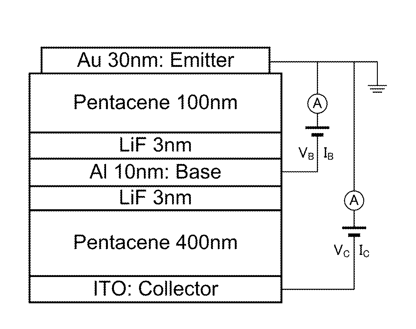
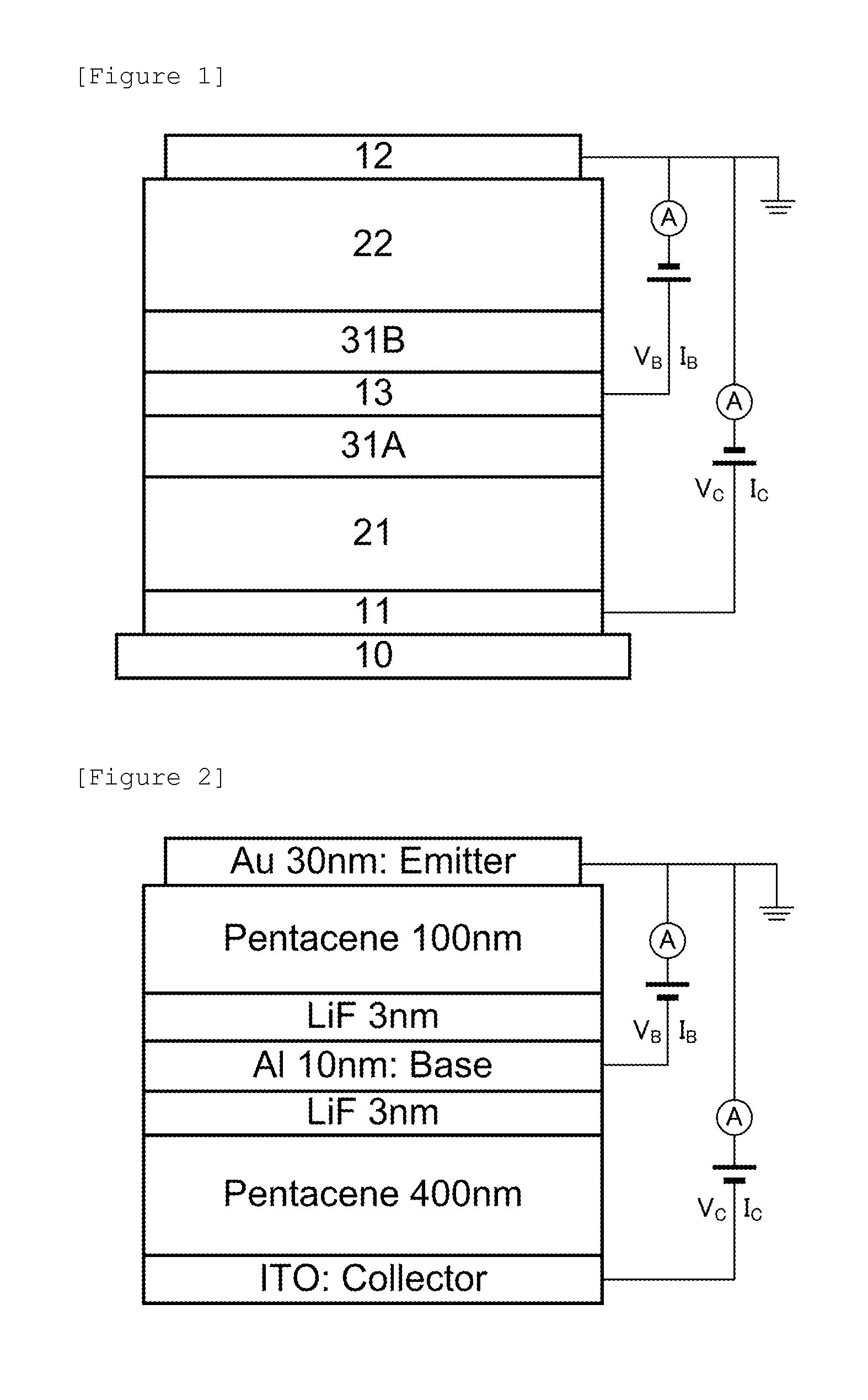
Current Transmission Promotion Layer: Collector Layer Side Thickness 1 nm / Emitter Layer Side Thickness 3 nm

[0095]Head-to-tail P3HT [regioregular-Poly(3-hexylthiophene-2,5-diyl)] was dissolved in toluene, and a P3HT solution was prepared so that the concentration became 20 mg / mL. The obtained P3HT solution was applied on an ITO transparent substrate by a spin coater to form a collector layer (250 nm). Next, a current transmission promotion layer comprising lithium fluoride (LiF), the current transmission promotion layer having a thickness of 1.0 nm was formed thereon, and further a base electrode layer comprising aluminum, the base electrode layer having an average thickness of 10 nm was formed by a vacuum deposition method. Thereafter, heat treatment was conducted at 150° C. under the atmospheric pressure for 1 hour to form an oxidized film layer (dark current suppression layer) on the surface of the aluminum electrode. Next, a current transmission promotion layer comprising lithium...

example 2

Current Transmission Promotion Layer: Collector Layer Side Thickness 0.6 nm / Emitter Layer Side Thickness 1 nm

[0097]Head-to-tail P3HT [regioregular-Poly(3-hexylthiophene-2,5-diyl)] was dissolved in toluene, and a P3HT solution was prepared so that the concentration became 20 mg / mL. The obtained P3HT solution was applied on an ITO transparent substrate by a spin coater to form a collector layer (250 nm). Next, a current transmission promotion layer comprising lithium fluoride (LiF), the current transmission promotion layer having a thickness of 0.6 nm was formed thereon, and further a base electrode layer comprising aluminum, the base electrode layer having an average thickness of 10 nm was formed by the vacuum deposition method. Thereafter, heat treatment was conducted at 150° C. under the atmospheric pressure for 1 hour to form an oxidized film layer (dark current suppression layer) on the surface of the aluminum electrode. Next, a current transmission promotion layer comprising lit...

example 3

Current Transmission Promotion Layer: Collector Layer Side Thickness 0.6 nm / Emitter Layer Side Thickness 3 nm

[0099]Head-to-tail P3HT [regioregular-Poly(3-hexylthiophene-2,5-diyl)] was dissolved in toluene, and a P3HT solution was prepared so that the concentration became 20 mg / mL. The obtained P3HT solution was applied on an ITO transparent substrate by a spin coater to form a collector layer (250 nm). Next, a current transmission promotion layer comprising lithium fluoride (LiF), the current transmission promotion layer having a thickness of 0.6 nm was formed thereon, and further a base electrode layer comprising aluminum, the base electrode layer having an average thickness of 10 nm was formed by the vacuum deposition method. Thereafter, heat treatment was conducted at 150° C. under the atmospheric pressure for 1 hour to form an oxidized film layer (dark current suppression layer) on the surface of the aluminum electrode. Next, a current transmission promotion layer comprising lit...


PUM


Abstract

The present invention provides a transistor element having a laminated structure, the laminated structure comprising a sheet-like base electrode being arranged between an emitter electrode and a collector electrode; at least one p-type organic semiconductor layer being provided on each of the surface and the back sides of the base electrode; and a current transmission promotion layer being formed, on each of the surface and back sides of the base electrode, between the base electrode and the p-type organic semiconductor layer or layers provided on each of the surface and back sides of the base electrode. According to the present invention, it becomes possible to provide a transistor element (MBOT) that is, in particular, stably supplied through a simple production process, has a structure capable of being mass-produced, and has a large current modulation effect and an excellent ON / OFF ratio at a low voltage in the emitter electrode and the collector electrode.

Description

TECHNICAL FIELD[0001]The present invention relates, in particular, to a transistor element that exhibits an excellent current modulation property, and, in more detail, to a transistor element that is excellent in current amplification factor to perform large current modulation with a low voltage capable of driving an organic EL display or the like.BACKGROUND ART[0002]In recent years, the spread of thin-type TVs and laptops has been progressing, and the performance requirements for display devices such as a liquid crystal display, an organic EL display, and electronic paper have been desired to be higher. Furthermore, the display devices are further becoming finer, smaller, and thinner with the spread of high-function cellular phones and tablet-type terminal devices. A field effect transistor (Field Effect Transistor: FET) has been used for driving such display elements. Currently, FETs using silicon that is an inorganic material have been extensively used, however displays using an ...

Claims


Application Information

Patent Timeline
Patent Type & Authority Applications(United States)
IPC IPC(8): H01L51/05H01L51/10
CPCH01L51/0504H01L2251/301H01L51/105H10K85/113H10K2102/103H10K10/43H10K10/46H10K10/00H10K10/84H10K2102/00
Inventor NAKAYAMA, KEN-ICHIKIDO, JUNJIAKIBA, RYOTAROOGUMA, NAOMIHIRATA, NAOKI
Owner DAINICHISEIKA COLOR & CHEM MFG CO LTD
Why Eureka
Try Eureka