Method of forming surface protrusions on an article and the article with the protrusions attached

a surface protrusion and protrusion technology, applied in the direction of soldering apparatus, manufacturing tools, instruments, etc., can solve the problems of high cost, difficult to achieve the precision of the probe tip for probing ultra-fine pitch pads, and difficult to achieve the necessary probe tip precision. , to achieve the effect of simple bumping method

Active Publication Date: 2015-08-27
IBM CORP
View PDF2 Cites 13 Cited by
  • Summary
  • Abstract
  • Description
  • Claims
  • Application Information

AI Technical Summary

Benefits of technology

[0011]A feature of the invention is a simple bumping method for forming protrusions on densely populated chip pads one or both sides of integrated circuit (IC) chips;
[0012]Another feature of the invention is a simple bumping method for forming micro-pillars on densely populated chip pads one or both sides of integrated circuit (IC) chips;
[0013]Yet another feature of the invention is a simple bumping method for forming solder bumps on densely populated chip pads one or both sides of integrated circuit (IC) chips;

Problems solved by technology

Testing these tightly packed pads with or without solder balls requires very fine, delicate, tightly-packed test probes.
Achieving necessary probe tip precision for probing ultra-fine pitch pads has proven very difficult, and therefore, expensive.

Method used


Image

  • Method of forming surface protrusions on an article and the article with the protrusions attached
  • Method of forming surface protrusions on an article and the article with the protrusions attached
  • Method of forming surface protrusions on an article and the article with the protrusions attached

Examples


Embodiment Construction

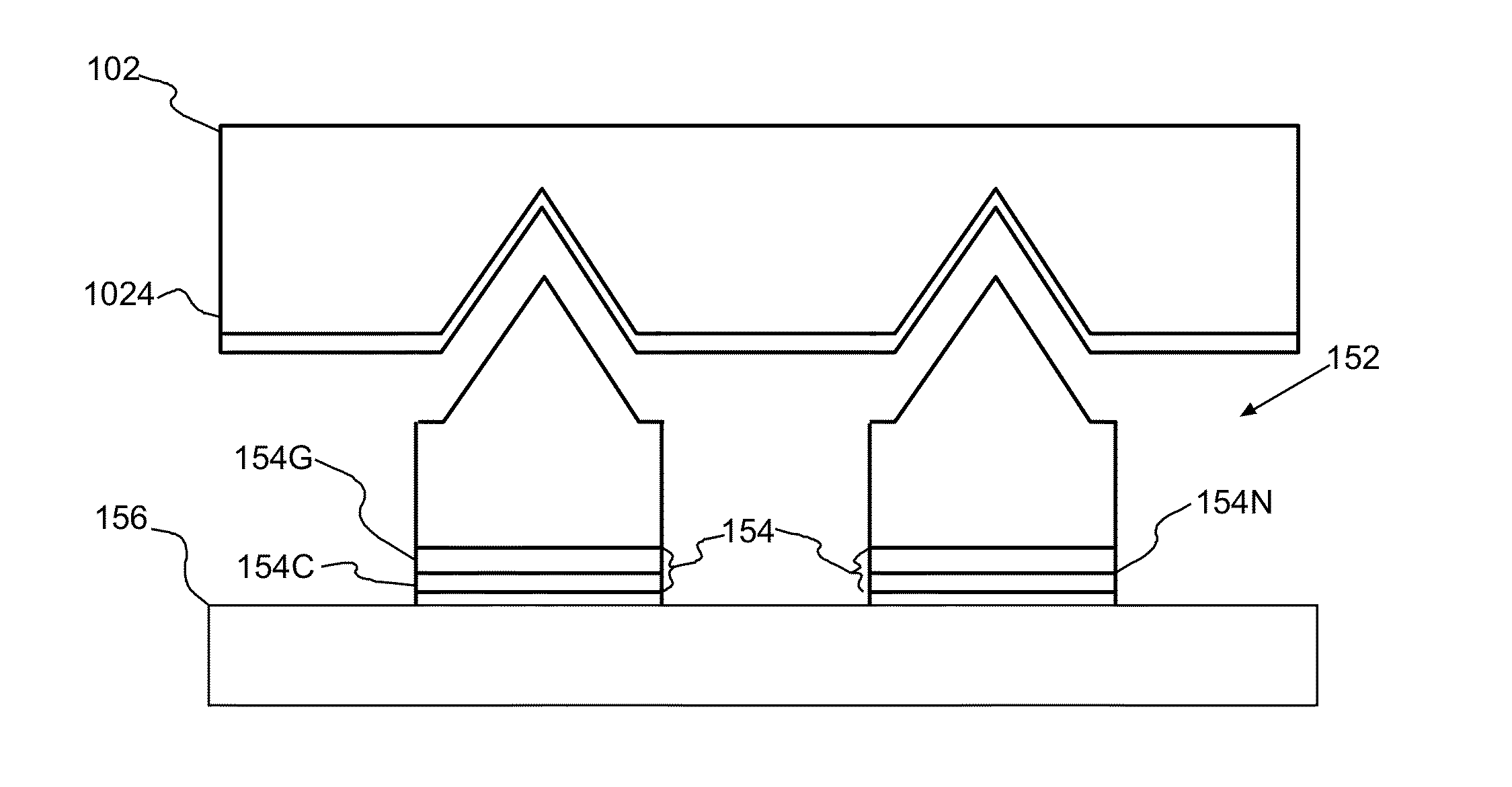
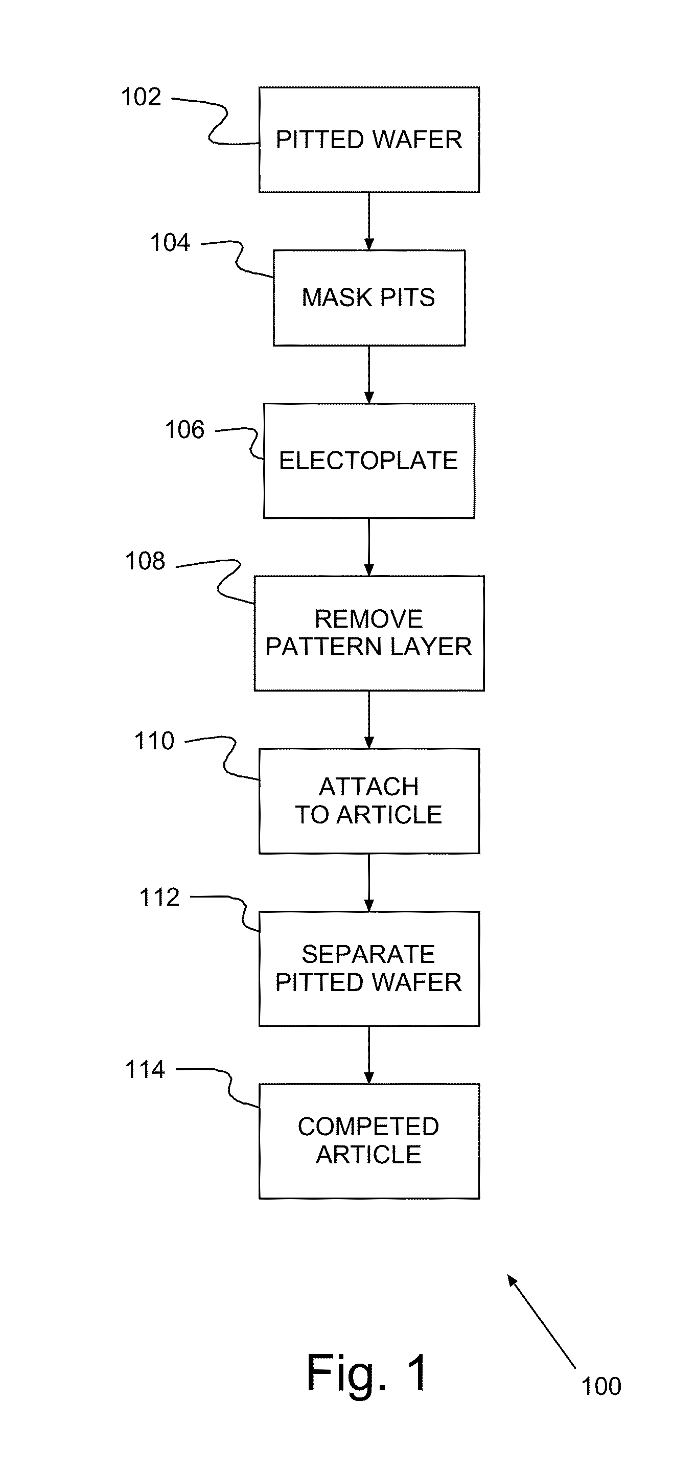
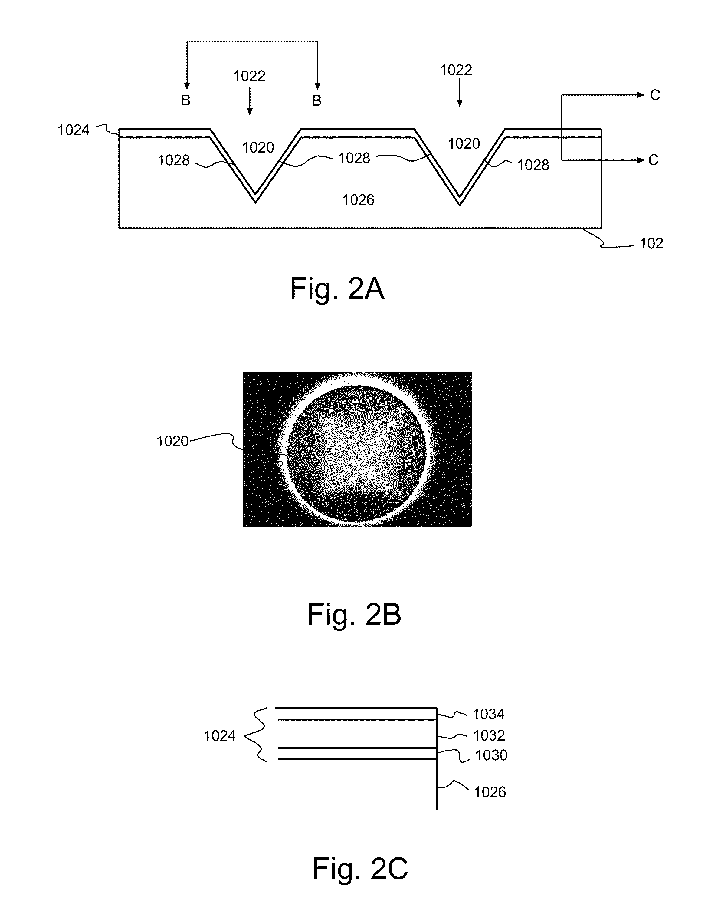
[0026]Turning now to the drawings and, more particularly, FIG. 1 shows an example of a method 100 of forming surface protrusions, e.g., test probes, solder bumps, micro pillars and / or cantilevered membranes, on an article according to a preferred embodiment of the present invention. The surface protrusions are electroplated to a low adhesion surface layer on a template or mold wafer 102, attached to the article and the template wafer 102 is removed. The low adhesion surface layer makes separating the template wafer 102 from the completed article easy.

[0027]Previously, using a low adhesion material, e.g., a native oxide on a titanium (Ti) layer or multi-layer, as a base for electroplating had made it difficult to initiate uniform nucleation and provided unstable results. Nucleates frequently fell in to the electroplating solution, causing difficult and non-uniform nucleation. Subsequently in post-plating cleaning steps, the larger deposition film / structure may detach prematurely (e.g...


PUM


Abstract

A method of forming surface protrusions on an article, and the article with the protrusions attached. The article may be an Integrated Circuit (IC) chip, a test probe for the IC chip or any suitable substrate or nanostructure. The surface protrusions are electroplated to a template or mold wafer, transferred to the article and easily separated from the template wafer. Thus, the attached protrusions may be, e.g., micro-bumps or micro pillars on an IC chip or substrate, test probes on a probe head, or one or more cantilevered membranes in a micro-machine or micro-sensor or other micro-electro-mechanical systems (MEMS) formed without undercutting the MEMS structure.

Description

CROSS REFERENCE TO RELATED APPLICATION[0001]The present invention is a divisional of U.S. patent application Ser. No. 14 / 187,237 (Attorney Docket No. YOR920130799US1), “METHOD OF FORMING SURFACE PROTRUSIONS ON AN ARTICLE AND THE ARTICLE WITH THE PROTRUSIONS ATTACHED” to Bing Dang et al., filed Feb. 22, 2014, assigned to the assignee of the present invention and incorporated herein by reference.BACKGROUND OF THE INVENTION[0002]1. Field of the Invention[0003]The present invention is related to semiconductor device manufacturing and more particularly to forming protrusions on an article, such as a semiconductor integrated circuit (IC) chip.[0004]2. Background Description[0005]Typical semiconductor integrated circuit (IC) chips have layers stacked such that layer features overlay one another to form individual devices and connect devices together. ICs are mass produced by forming an array of chips on a thin semiconductor wafer. Each array location is known as a die and each die may harb...

Claims


Application Information

Patent Timeline
Patent Type & Authority Applications(United States)
IPC IPC(8): G01R1/073B81B3/00G01R31/26
CPCG01R1/0735B81B2201/02B81B3/00G01R31/2607H01L2224/11003H01L2224/11849H01L2924/14H01L24/05H01L24/06H01L24/13H01L2224/0401H01L2224/04042H01L2224/05082H01L2224/05147H01L2224/05155H01L2224/05644H01L2224/06131H01L2224/06135H01L2224/06136H01L2224/13082H01L2224/13083H01L2224/13111H01L2224/13147H01L2224/73207H01L2224/111H01L2224/1112H01L2924/381B81C1/00626B81B2203/0118B81B2203/0127H01L2224/1366H01L2224/11334H01L2224/13017H01L2224/13019H01L2224/13564H01L2224/1357H01L2224/136H01L2224/13655H01L2224/13657H01L2224/13663B23K35/262B23K35/0244B23K35/025B23K2101/36B23K2101/40H01L24/11H01L2924/01029H01L2924/01022H01L2924/014H01L2924/01028H01L2924/00012H01L2924/00014H01L2924/01047H01L2924/01104B23K35/00
Inventor DANG, BINGKNICKERBOCKER, JOHNLIU, YANGMASON, MAURICEROMANKIW, LUBOMYR T.
Owner IBM CORP
Why Eureka
Try Eureka