Piezoresistive MEMS sensor
a sensor and mems technology, applied in the field of mems devices, can solve the problems of large variation in the sensor, affecting the sensor sensitivity, and increasing the cos
- Summary
- Abstract
- Description
- Claims
- Application Information
AI Technical Summary
Benefits of technology
Problems solved by technology
Method used
Image
Examples
working examples
Working Example 1
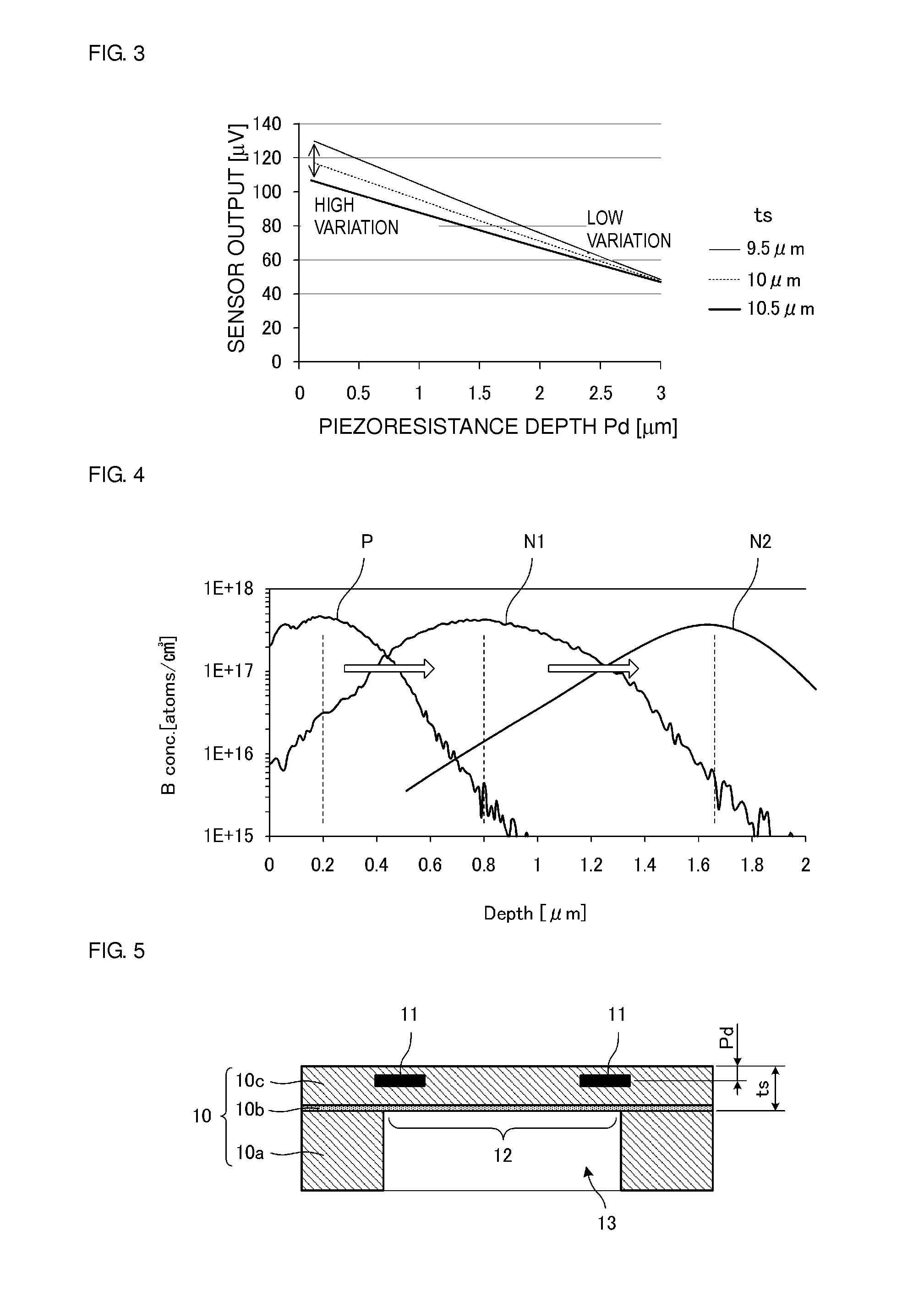
[0036]FIG. 5 is a cross-sectional view of a pressure sensor according to Working Example 1. This pressure sensor is constituted by a SOI substrate that preferably is a Si substrate 10a, a SiO2 layer 10b, and a surface Si film 10c. An opening portion 13 is formed in the Si substrate 10a preferably through etching, and the displacement portion 12 having a membrane structure is defined by the surface Si film 10c and the SiO2 layer 10b in this area. The piezoresistive element 11 is formed in the displacement portion 12 preferably through ion injection. The displacement portion 12 bends in response to a pressure to be detected and a resistance value of the piezoresistive element changes in response thereto.
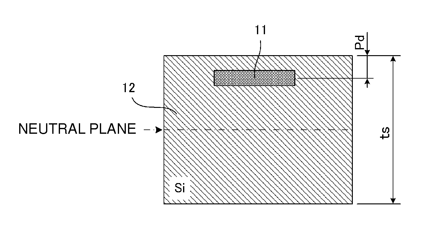
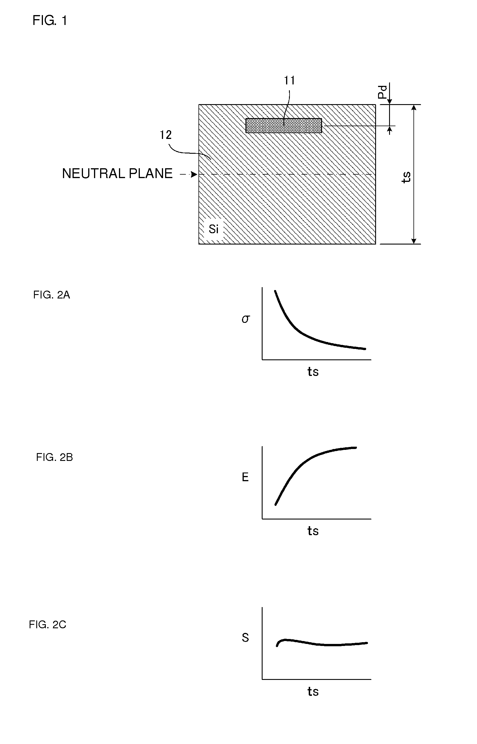
[0037]Here, the thickness dimension is of the membrane-structure displacement portion 12 preferably is not less than about 1 μm and not greater than about 10 μm, and the position (depth) Pd of the peak of the impurity concentration of the piezoresistive element 11 is g...
working example 2
[0039]FIG. 7 is a cross-sectional view of a pressure sensor according to Working Example 2. In this example, a protective film 14 is formed on the surface of the Si film 10c on which the piezoresistive element 11 is formed. The rest of the configuration is preferably the same as in the pressure sensor illustrated in FIG. 5.
[0040]FIG. 8A, FIG. 8B, FIG. 8C, and FIG. 8D are cross-sectional views illustrating a non-limiting example of a process for manufacturing the pressure sensor illustrated in FIG. 7. First, as illustrated in FIG. 8A, an SOI substrate 10 formed of the Si substrate 10a, the SiO2 layer 10b, and the surface Si film 10c is prepared. Next, as illustrated in FIG. 8B, the piezoresistive element 11 is formed through ion injection from the surface Si film 10c. Then, as illustrated in FIG. 8C, the protective film 14 constituted by a Si oxide film or a Si nitride film is formed on the surface through thermal oxidization or CVD. Then, as illustrated in FIG. 8D, the opening porti...
working example 3
[0041]FIG. 9 is a cross-sectional view of an accelerometer according to Working Example 3. This accelerometer includes a SOI substrate that includes the Si substrate 10a, the SiO2 layer 10b, and the surface Si film 10c. The opening portion 13 is formed in the Si substrate 10a preferably through etching, and the displacement portion 12 having a beam structure is defined by the surface Si film 10c and the SiO2 layer 10b in this area. One side of the Si substrate 10a connected by the beam-structure displacement portion 12 defines and functions as an anchoring portion, and the other side of the Si substrate 10a acts as a weight. The piezoresistive element 11 is formed in the displacement portion 12 preferably through ion injection. The displacement portion 12 bends in response to an acceleration to be detected and a resistance value of the piezoresistive element changes in response thereto.
[0042]Here, the thickness dimension is of the membrane-structure displacement portion 12 preferabl...
PUM
| Property | Measurement | Unit |
|---|---|---|
| thickness | aaaaa | aaaaa |
| thickness | aaaaa | aaaaa |
| thickness | aaaaa | aaaaa |
Abstract
Description
Claims
Application Information
 - R&D
- Intellectual Property
- Life Sciences
- Materials
- Tech Scout
- Unparalleled Data Quality
- Higher Quality Content
- 60% Fewer Hallucinations
Browse by: Latest US Patents, China's latest patents, Technical Efficacy Thesaurus, Application Domain, Technology Topic, Popular Technical Reports.
© 2025 PatSnap. All rights reserved.Legal|Privacy policy|Modern Slavery Act Transparency Statement|Sitemap|About US| Contact US: help@patsnap.com


