Eureka AIR delivers breakthrough ideas for toughest innovation challenges, trusted by R&D personnel around the world.

Liquid crystal display device

Active Publication Date: 2015-08-20
DAINIPPON INK & CHEM INC
View PDF2 Cites 9 Cited by
  • Summary
  • Abstract
  • Description
  • Claims
  • Application Information

AI Technical Summary

Benefits of technology

The liquid crystal display device described in this patent prevents issues like a decrease in voltage holding ratio and an increase in ion density in the liquid crystal layer by using a particular liquid crystal composition and a color filter. It also prevents display defects like missing dots, alignment variation, and ghosting.

Problems solved by technology

A liquid crystal material constituting a liquid crystal layer has been subject to strict impurity control since impurities remaining in the material will significantly affect electrical properties of display devices.
Accordingly, it is not proper to assume that a color filter layer and a liquid crystal layer are completely isolated from each other and it is possible that display defects such as missing dots, alignment variation, and ghosting would occur due to a decrease in voltage holding ratio (VHR) and an increase in ion density (ID) of the liquid crystal layer caused by impurities migrating from the color filter layer through the alignment film and the transparent electrode.
However, these techniques are not much different from simply decreasing the amount of impurities contained in the pigment and the improvements brought about thereby are insufficient for resolving display defects under current situations of advancement in pigment purification techniques.
This is not sufficient for resolving display defects of recent advanced liquid crystal display elements.
It is known that the water soluble matter in and the electrical conductivity of a pigment affect the antirust effect of antirust paints and discharge properties of inkjet inks (PTL 5 and PTL 6); however, the effect of a combination of the water soluble matter and the electrical conductivity of the pigment and the structure of the liquid crystal material constituting the liquid crystal layer has not been known, and the problem of display defects in advanced liquid crystal display devices has not been resolved.

Method used


Image

  • Liquid crystal display device
  • Liquid crystal display device
  • Liquid crystal display device

Examples


examples

[0128]Some of the best embodiments of the present invention are described in detail by using Examples below. These examples do not limit the present invention. For the compositions of Examples and Comparative Examples, “%” means “% by mass”.

[0129]The physical properties of the liquid crystal composition are referred to as follows:

TN-I: nematic phase-isotropic liquid phase transition temperature (° C.), liquid crystal phase upper limit temperature

Δ∈: dielectric anisotropy

Δn: refractive index anisotropy

η: viscosity (mPa·s) at 20° C.

dgap: gap (μm) between a first substrate and a second substrate of a cell

VHR: voltage holding (%) ratio at 70° C.

(A liquid crystal composition was placed in a cell having a thickness of 3.5 μm and measurement was conducted under application of 5 V at a frame time of 200 ms and a pulse width of 64 μs. The percentage of the voltage observed in the measurement to the initial application voltage was assumed to be the voltage holding ratio.)

ID: ion density (pC / c...

examples 1 to 4

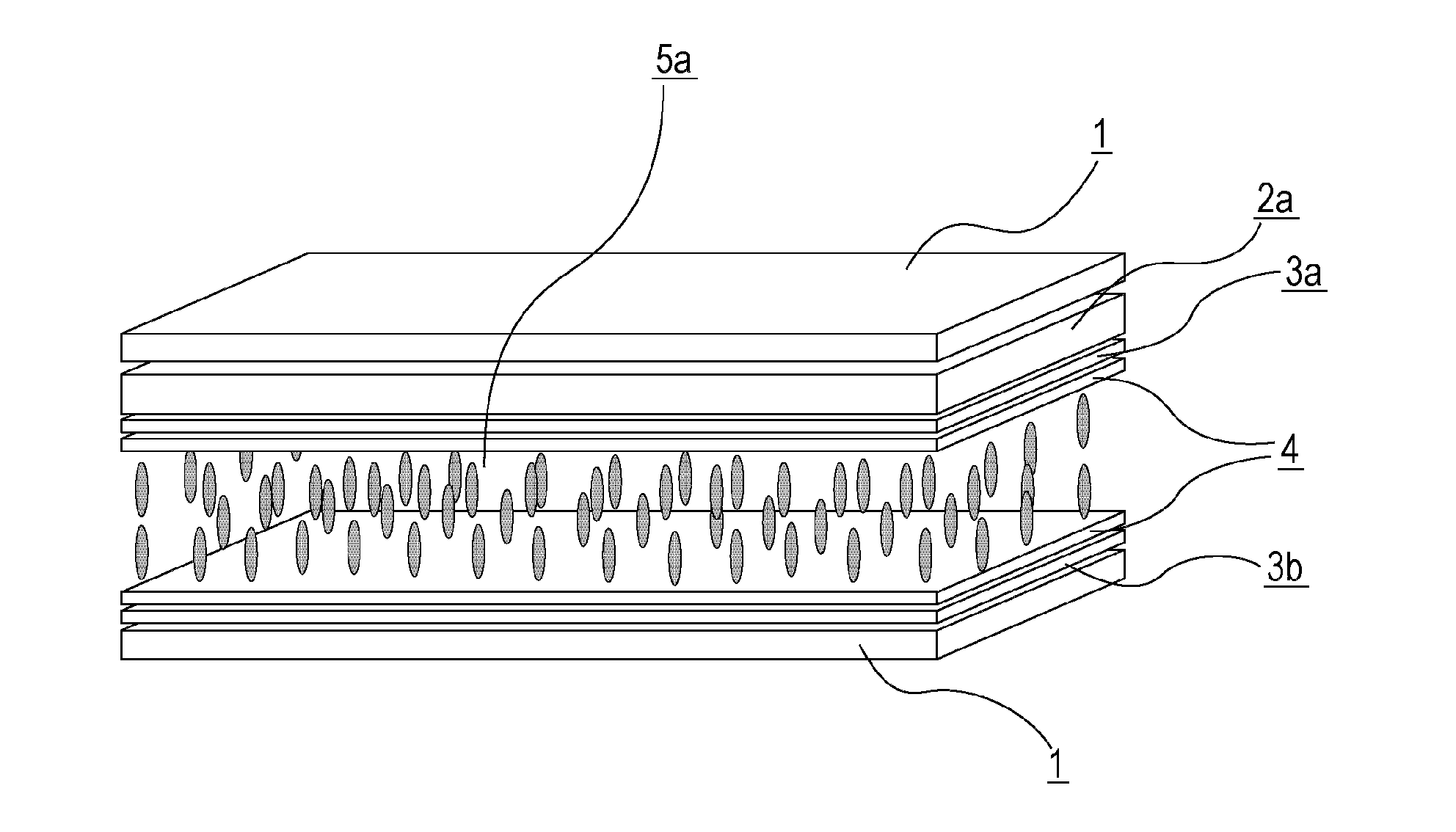
[0165]Electrode structures were formed on the first and second substrates. A vertical alignment film was formed on each of the surfaces that oppose each other and subjected to weak rubbing treatment to prepare a VA cell. A liquid crystal composition 1 having negative dielectric anisotropy indicated in Table 9 was placed between the first substrate and the second substrate. Next, color filters 1 to 4 indicated in Table 8 were used to produce liquid crystal display devices of Examples 1 to 4 (dgap=3.5 μm, alignment film: SE-5300). The VHR and ID of the liquid crystal display devices were measured. Ghosting evaluation was also conducted on the liquid crystal display devices. The results are indicated in Table 10.

TABLE 9Liquid crystal composition 10d1-Cy-Cy-3203-Cy-Cy-2153-Cy-Ph—O150d1-Cy-1O—Ph5—O1-Cy-2110d1-Cy-1O—Ph5—O1-Cy-3110d1-Cy-1O—Ph5—O1-Cy-4110d1-Cy-1O—Ph5—O1-Cy-5110d1-Cy-Cy-1O—Ph5—O3d040d1-Cy-Cy-1O—Ph5—O4d040d1-Cy-1O—Ph5—O1-Cy-Cy-240d1-Cy-1O—Ph5—O1-Cy-Cy-34Total (%)100Tni / ° C.82...

examples 5 to 12

[0173]Liquid crystal display devices of Examples 5 to 12 were prepared as in Example 1 by using negative dielectric anisotropy liquid crystals indicated in Table 17 and the color filters 1 to 4 indicated in Table 8. The VHR and ID thereof were measured. Ghosting evaluation was conducted on the liquid crystal display devices. The results are indicated in Tables 18 and 19.

TABLE 17Liquid crystalLiquid crystalcomposition 2composition 33-Cy-1O—Ph5—O211115-Cy-1O—Ph5—O210100d1-Cy-Cy-3200d1-Cy-Cy-5200d3-Cy-Cy-310103-Cy-1 = 1-Cy-310100d1-Cy-1O—Ph5—O1-Cy-350d1-Cy-Cy-1O—Ph5—O3d050d1-Cy-Cy-1O—Ph5—O4d052-Cy-Cy-1O—Ph5—O2553-Cy-Cy-1O—Ph5—O212124-Cy-Cy-1O—Ph5—O2550d1-Cy-1O—Ph5—O1-Cy-Cy-1d0120d1-Cy-1O—Ph5—O1-Cy-Cy-250d1-Cy-1O—Ph5—O1-Cy-Cy-32Total (%)100100Tni / ° C.79.678.9Δn(20° C.)0.0740.075η20 / mPa · s17.818.2Δε(20° C.)−4.8−4.8

TABLE 18Example 5Example 6Example 7Example 8Liquid crys-Liquid crys-Liquid crys-Liquid crys-Liquid crys-tal compo-tal compo-tal compo-tal compo-tal compo-sitionsition 2sition ...


PUM

PropertyMeasurementUnit
Fractionaaaaaaaaaa
Percent by massaaaaaaaaaa

Abstract

The present invention relates to a liquid crystal display device that uses a particular liquid crystal composition and a color filter that uses a particular pigment.The present invention provides a liquid crystal display device that prevents a decrease in voltage holding ratio (VHR) and an increase in ion density (ID) of a liquid crystal layer and resolves the problems of display defects, such as missing dots, alignment variation, and ghosting.Since the liquid crystal display device of the present invention prevents a decrease in voltage holding ratio (VHR) and an increase in ion density (ID) of a liquid crystal layer and resolves the problems of display defects, such as ghosting, it is particularly useful for active matrix drive VA-mode and PSVA-mode liquid crystal display devices and can be applied to liquid crystal display devices such as liquid crystal televisions, monitors, cellular phones, and smart phones.

Description

TECHNICAL FIELD[0001]The present invention relates to a liquid crystal display device.BACKGROUND ART[0002]Liquid crystal display devices have come to be used in watches, calculators, various home electric appliances, measurement instruments, automobile panels, word processors, electronic organizers, printers, computers, televisions, and other applications. Representative examples of the liquid crystal display mode include twisted nematic (TN) mode, super twisted nematic (STN) mode, dynamic scattering (DS) mode, guest / host (GH) mode, in-plane-switching (IPS) mode, optically compensated bend (OCB) mode, electrically controlled birefringence (ECB) mode, vertical alignment (VA) mode, color super homeotropic (CSH) mode, and ferroelectric liquid crystals (FLC). As for the driving mode, multiplex driving has become popular replacing the conventional static driving, and the mainstream mode is a simple matrix mode, and recently, an active matrix (AM) mode in which driving is performed by usi...

Claims


Application Information

Patent Timeline
IPC IPC(8): C09K19/30G02F1/1335C09K19/56G02F1/1334C09K19/34C09K19/32
CPCC09K19/3001C09K19/3402C09K19/322C09K19/3003C09K19/56G02F1/1334C09K2019/3078G02F1/133514C09K2019/3425C09K2019/3004C09K2019/3009C09K2019/301C09K2019/3016G02F1/133512C09K2019/122C09K2019/123C09K2019/305C09K2019/325C09K2019/523C09B67/0033C09B67/009G02B5/201G02F1/133397C09K19/20C09K2019/0448C09K2019/0466
Inventor KANEOYA, MASAKAZUTAKEUCHI, KIYOFUMIFUNAKURA, SEIJIOSHIUMI, ISAOSHIMADA, KATSUNORI
Owner DAINIPPON INK & CHEM INC
Why Eureka
Eureka Blog
Learn More