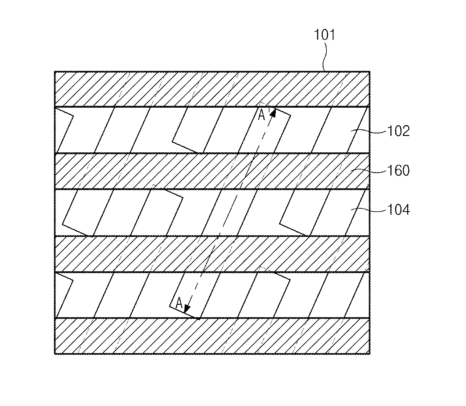
Semiconductor device and method for forming the same
a semiconductor device and a technology of a semiconductor device, applied in the direction of semiconductor devices, basic electric elements, electrical appliances, etc., can solve the problems of reducing productivity, reducing the gidl characteristics of the whole semiconductor device, and reducing the contact resistance. , to achieve the effect of preventing the characteristics and reliability of the device from being deteriorated, improving the gidl characteristics of the buried gate, and reducing contact resistan
- Summary
- Abstract
- Description
- Claims
- Application Information
AI Technical Summary
Benefits of technology
Problems solved by technology
Method used
Image
Examples
first embodiment
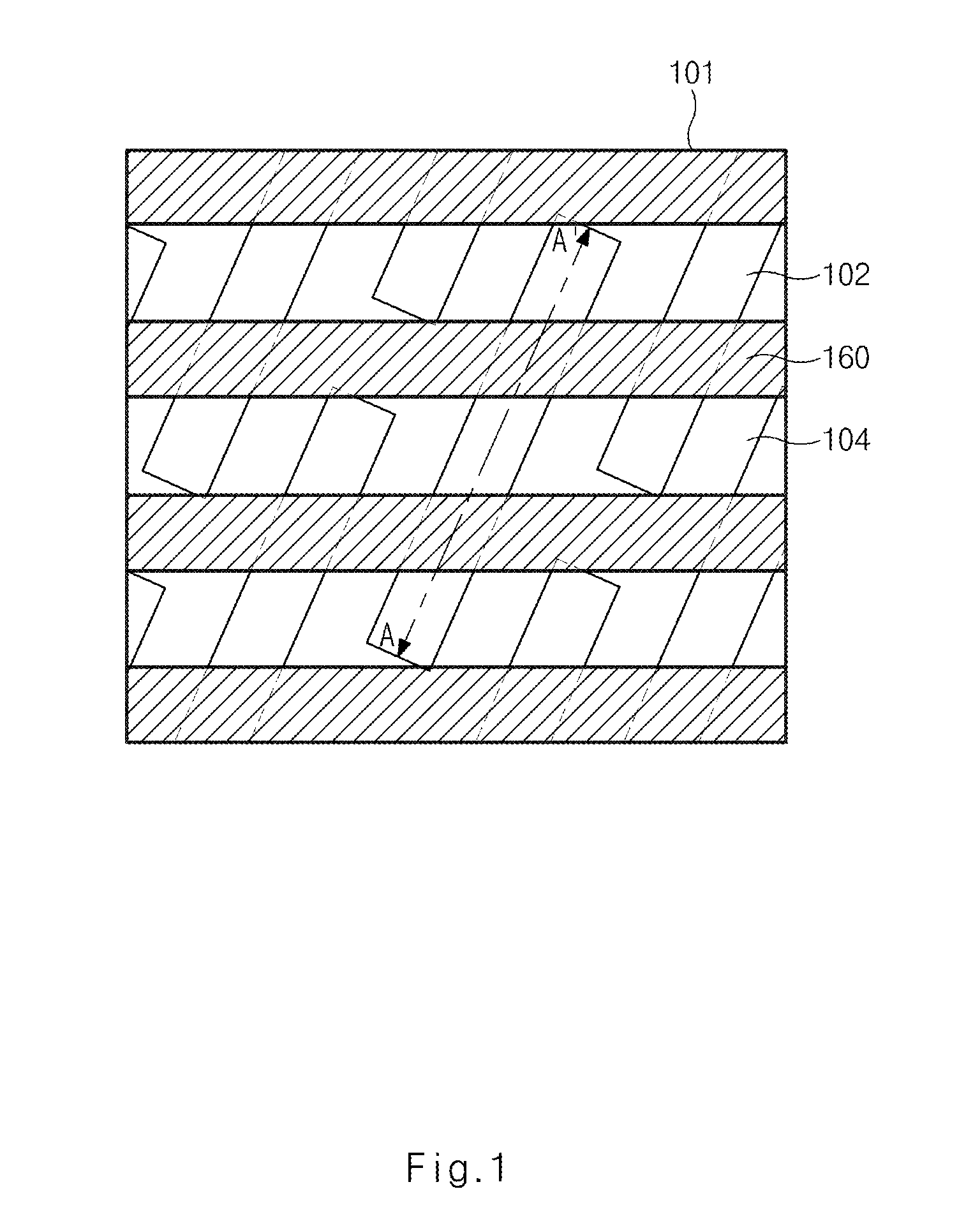
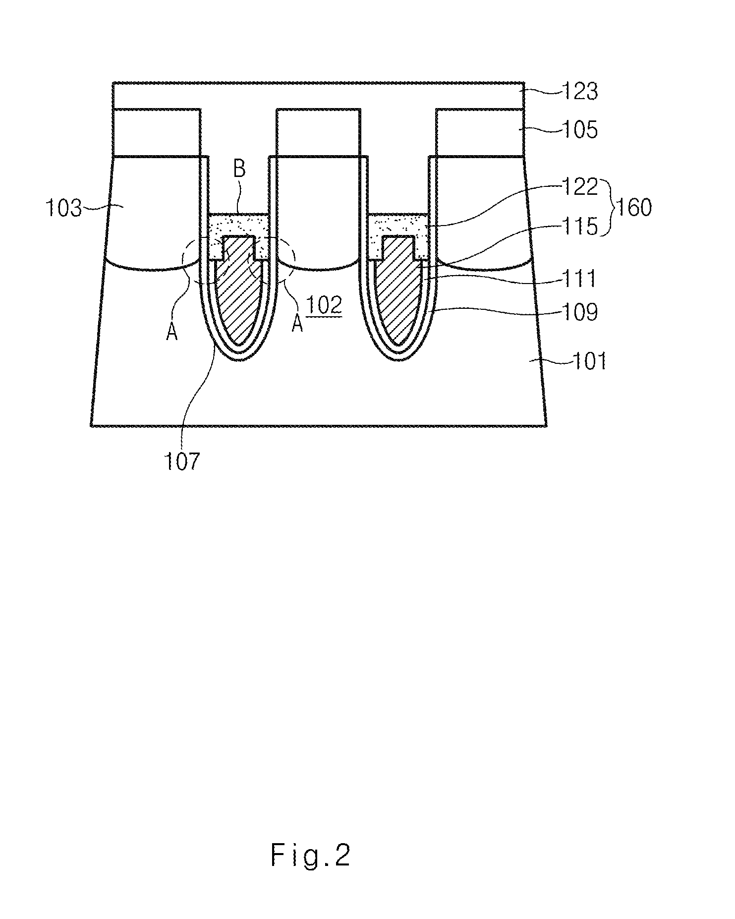
[0026]FIG. 2 is a cross-sectional view illustrating a semiconductor device taken along the line A-A′ of FIG. 1 according to a
[0027]Referring to FIG. 2, a trench 107 is formed in the active region 102, and a gate insulation film 109 and a barrier metal film 111 are sequentially stacked in the trench 107, such that a semiconductor device according to an embodiment can be formed. A first gate electrode 115 is formed over the barrier metal film 111, and a second gate electrode 122 is formed over the first gate electrode 115.
[0028]The embodiment of FIG. 2 shows a buried gate 160 having two-part gate electrode structure that includes second electrode 122 disposed over a first gate electrode 115. Side portions of the second gate electrode 122 are disposed between a junction region 103 of the semiconductor substrate 101 and the first gate electrode 115. As indicated in area “A” of FIG. 2, lower surfaces of second gate electrode 115 are level with lower boundaries of junction region 103. The...
second embodiment
[0035]FIG. 3 is a cross-sectional view illustrating a semiconductor device according to a
[0036]Referring to FIG. 3, a semiconductor device according to a second embodiment includes a buried gate 260 buried in the semiconductor substrate 101. The buried gate 260 includes a gate insulation film 109 and a barrier metal film 111 sequentially formed in a trench, a first gate electrode 215 formed over the barrier metal film 111, and a second gate electrode 222 formed over the first gate electrode 215.
[0037]Referring to FIG. 3, the top surface of the first gate electrode 215 extends between side surfaces of barrier metal film 111, and a second gate electrode 222 formed of a polycide layer extends between side surfaces of gate insulation film 109 and is disposed over first gate electrode 215. Unlike the first gate electrode 115 of the first embodiment, the second gate electrode 215 of the second embodiment does not have lower side portions interposed between first gate electrode 115 and sid...
third embodiment
[0039]FIG. 6 is a cross-sectional view illustrating a semiconductor device taken along the line A-A′ of FIG. 1 according to a
[0040]Referring to FIG. 6, the buried gate 360 includes a gate insulation film 109 and a barrier metal film 111 sequentially formed in a trench, a first gate electrode 315 formed over the barrier metal film 111, and a second gate electrode 322 formed between the first gate electrode 315 and the sidewalls of the trench 107. A space is between the first gate electrode 315 and sidewalls of the trench 107. A barrier metal film 111 is filled a lower portion of the space and the second gate electrode 322 disposed in upper portion of the space between the first gate electrode 315 and sidewalls of the trench 107. As described above, in embodiments, polysilicon formed by impurity implantation is silicided so that a polycide material is used as a second gate electrode.
[0041]In more detail, whereas a silicide material has the same workfunction as that of tungsten when po...
PUM
 Abstract
Description
Claims
Application Information
 - R&D
- Intellectual Property
- Life Sciences
- Materials
- Tech Scout
- Unparalleled Data Quality
- Higher Quality Content
- 60% Fewer Hallucinations
Browse by: Latest US Patents, China's latest patents, Technical Efficacy Thesaurus, Application Domain, Technology Topic, Popular Technical Reports.
© 2025 PatSnap. All rights reserved.Legal|Privacy policy|Modern Slavery Act Transparency Statement|Sitemap|About US| Contact US: help@patsnap.com


