
Epitaxial growth apparatus

a growth apparatus and growth tube technology, applied in the direction of crystal growth process, polycrystalline material growth, chemically reactive gas, etc., can solve the problems of uneven insufficient uniform temperature distribution within the wafer plane heated by the halogen lamp, and affecting the growth so as to prevent the deposition of by-products, enhance the uniform thickness of the epitaxial layer in the plane, and ensure mechanical strength

Active Publication Date: 2015-07-02
SUMCO CORP
View PDF2 Cites 5 Cited by
  • Summary
  • Abstract
  • Description
  • Claims
  • Application Information

AI Technical Summary

Benefits of technology

The present invention aims to solve issues in the production of epitaxial layers on wafers by reducing thickness unevenness and preventing by-products from adhering to the chamber. The technical effects of the invention include improved quality and efficiency in the production of epitaxial layers.

Problems solved by technology

However, according to the configuration of the conventional epitaxial growth apparatus, the temperature distribution within the wafer plane heated by the halogen lamps is not sufficiently uniform due to the effects of the reflection member.
Therefore, the epitaxial layer may be uneven in thickness.
Therefore, the temperature of the central portion of the upper dome tends to drop, and the problem is that by-products of silicon can easily adhere to the upper dome.
If the by-products are attached, the thermal radiation energy from the halogen lamps cannot easily pass through the upper dome.
As a result, the temperature in the central region of the wafer is more likely to drop, and the temperature distribution within the wafer plane becomes even more uneven.
The existence of the reflection member likely leads to unevenness of the in-plane temperature distribution of the wafer.

Method used


Image

  • Epitaxial growth apparatus
  • Epitaxial growth apparatus
  • Epitaxial growth apparatus

Examples


Embodiment Construction

[0030]Preferred embodiments of the present invention will be explained below in detail with reference to the accompanying drawings.

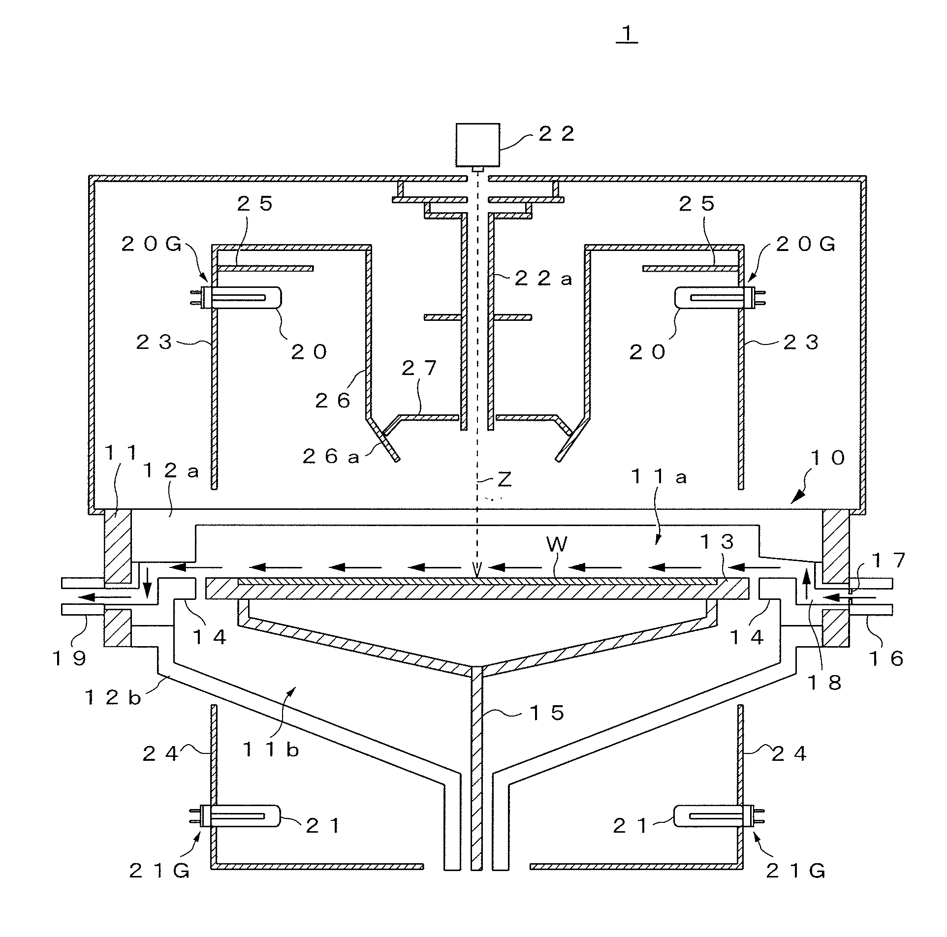
[0031]FIG. 1 is a schematic side cross-sectional view showing the configuration of an epitaxial growth apparatus 1 according to a preferred embodiment of the present invention.

[0032]As shown in FIG. 1, an epitaxial growth apparatus 1 is a single wafer-type apparatus that can process silicon wafers one by one. The epitaxial growth apparatus 1 includes a chamber 10 in which a wafer W is housed, and a susceptor 13 which supports the wafer W horizontally in the chamber 10 from a lower surface side thereof. The susceptor 13 is supported by a support shaft 15 in a rotatable manner. In one side portion of the chamber 10, a gas inlet 16, a baffle 17, and a rectifying member 18 are provided. In the other side portion opposite to the one side portion, a gas outlet 19 is provided. Incidentally, predetermined directions in the epitaxial growth apparatus 1 are define...


PUM

PropertyMeasurementUnit
temperatureaaaaaaaaaa
cylindrical shapeaaaaaaaaaa
optical axisaaaaaaaaaa

Abstract

Disclosed herein is an epitaxial growth apparatus for growing an epitaxial layer on a surface of a wafer. The apparatus includes: a chamber in which the wafer is housed; an upper lamp group that includes a plurality of heating lamps arranged in a ring above the chamber; a lower lamp group that includes a plurality of heating lamps provided below the chamber; a reflection member that is provided inside the ring of the upper lamp group, the reflection member having a substantially cylindrical shape; and an additional reflection member that is provided inside the reflection member, the additional reflection member including a reflection surface that is substantially parallel to the surface of the wafer. The additional reflection member is provided in such a way as to close at least part of an opening of a lower end portion of the reflection member.

Description

BACKGROUND OF THE INVENTION[0001]1. Field of the Invention[0002]The present invention relates to an epitaxial growth apparatus, and particularly to an epitaxial growth apparatus having a heating structure used to efficiently and evenly heat a wafer in a chamber.[0003]2. Description of Related Art[0004]An epitaxial growth apparatus is widely used as an apparatus for forming a single crystal layer (epitaxial layer) on the surface of a silicon wafer, for example. In a single wafer-type epitaxial growth apparatus, while a source gas is introduced into a camber in which one wafer is placed horizontally, heating is carried out to achieve a predetermined temperature, thereby growing an epitaxial layer.[0005]The wafer needs to be heated at a high temperature ranging from 1,000 to 1,200 degrees Celsius. Halogen lamps are used as the heating source. Many halogen lamps are arranged in an upper and a lower portion of the chamber. In the upper portion of the chamber, a pyrometer is provided to m...

Claims


Application Information

Patent Timeline
Patent Type & Authority Applications(United States)
IPC IPC(8): C30B25/10C30B25/08
CPCC30B25/08C30B25/10C30B29/06H01L21/67115
Inventor YOSHITAKE, KANOKAMOTO, KIMITAKASHOJI, HARUKI
Owner SUMCO CORP
Learn More