
Bilayer graphene tunneling field effect transistor

a field effect transistor and bilayer graphene technology, applied in the direction of semiconductor devices, basic electric elements, electrical apparatus, etc., can solve the problems of poor on-current/off-current ion/off ratio of field effect transistors using slg as active channels, inability to switch off, and limiting factors affecting the use of graphene in microelectronics for logic applications, etc., to achieve good control of the junction profile and the concentration of dopan

Active Publication Date: 2015-06-18
INTERUNIVERSITAIR MICRO ELECTRONICS CENT (IMEC VZW) +1
View PDF1 Cites 22 Cited by
  • Summary
  • Abstract
  • Description
  • Claims
  • Application Information

AI Technical Summary

Benefits of technology

The patent text describes a method to create a semiconductor device using a has steps to control the dopant concentration and the junction profile. This allows for the creation of highly controlled regions in the device without the need for chemical doping. The resulting device has improved performance and greater control over its properties.

Problems solved by technology

As a consequence, field effect transistors (FETs) using SLG as active channel exhibit a poor on-current / off current Ion / Ioff ratio (generally ˜10), and they cannot be switched off.
This is one of the main limiting factors hampering the use of graphene in microelectronics for logic applications.
The first approach (i.e. chemical doping), however, is not easily controlled as the dopants tend to spread non-uniformly on the BLG.
Furthermore, the dopant tends to migrate and interact with graphene, creating defects leading to device performance stability problems.
Also, the deposition of dopants is so far hardly compatible with typical CMOS process flows.
Also dopant profile engineering is not sufficient as, due to the weak nature of the interaction of graphene and adsorbates, it is very difficult to achieve homogeneous dopant profiles along the graphene.
With current state of the art it is very challenging to achieve steep shallow dopant profiles (and thus abrupt p-i-n junctions) which are necessary for sub-100 nm technologies.

Method used


Image

  • Bilayer graphene tunneling field effect transistor
  • Bilayer graphene tunneling field effect transistor
  • Bilayer graphene tunneling field effect transistor

Examples


Embodiment Construction

[0099]The present disclosure will be described with respect to particular embodiments and with reference to certain drawings but the disclosure is not limited thereto but only by the claims. The drawings described are only schematic and are non-limiting. In the drawings, the size of some of the elements may be exaggerated and not drawn on scale for illustrative purposes. The dimensions and the relative dimensions do not necessarily correspond to actual reductions to practice of the disclosure.

[0100]Moreover, the terms top, bottom, over, under and the like in the description and the claims are used for descriptive purposes and not necessarily for describing relative positions. The terms so used are interchangeable under appropriate circumstances and the embodiments of the disclosure described herein can operate in other orientations than described or illustrated herein.

[0101]Furthermore, the various embodiments, although referred to as “preferred” are to be construed as exemplary man...


PUM


Abstract

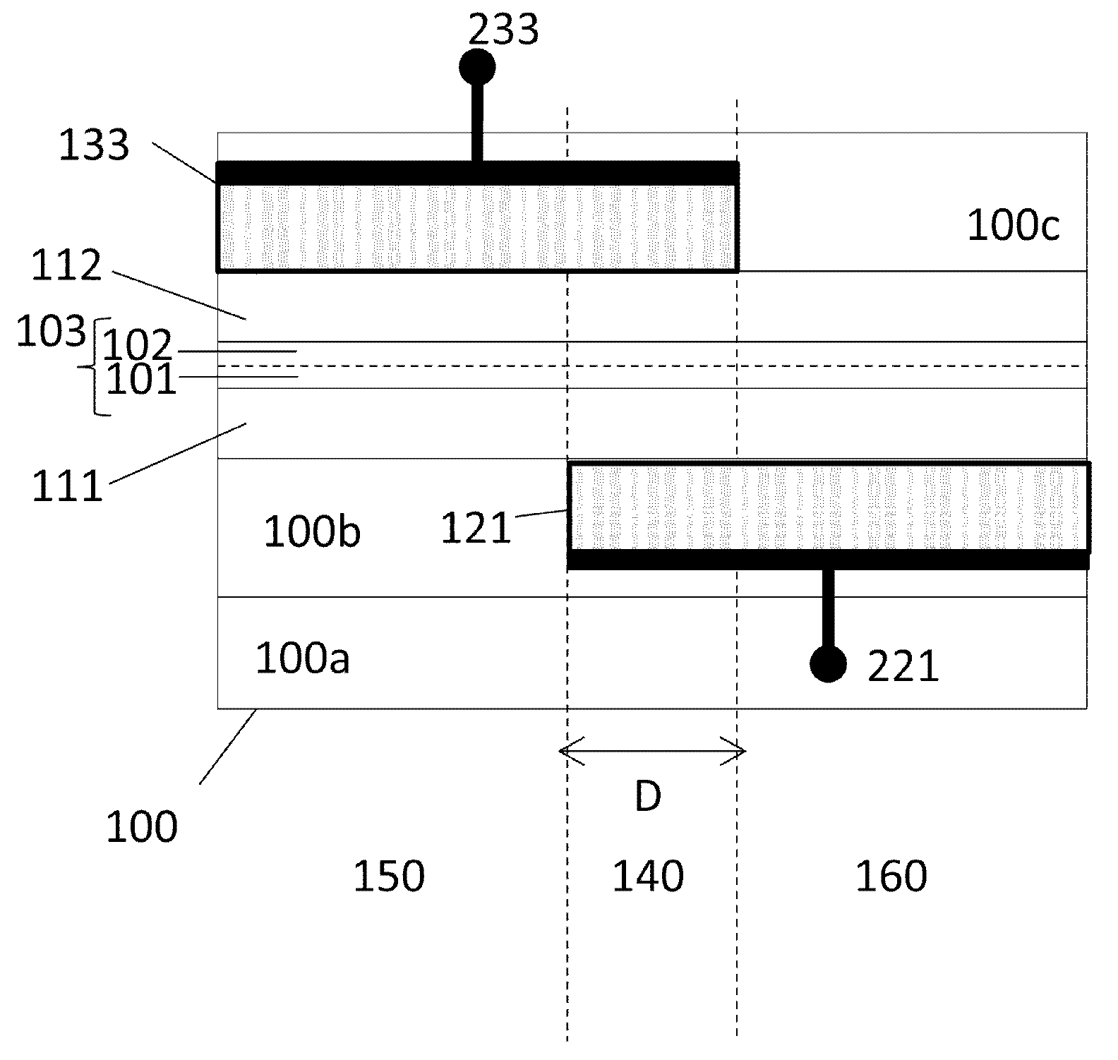
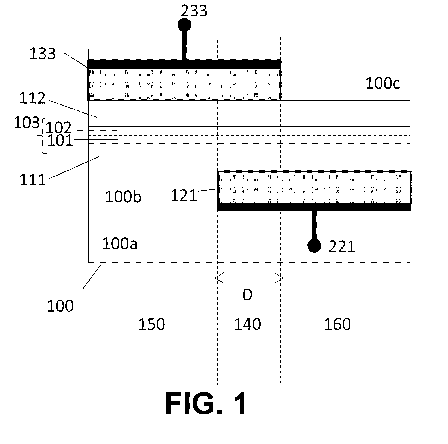
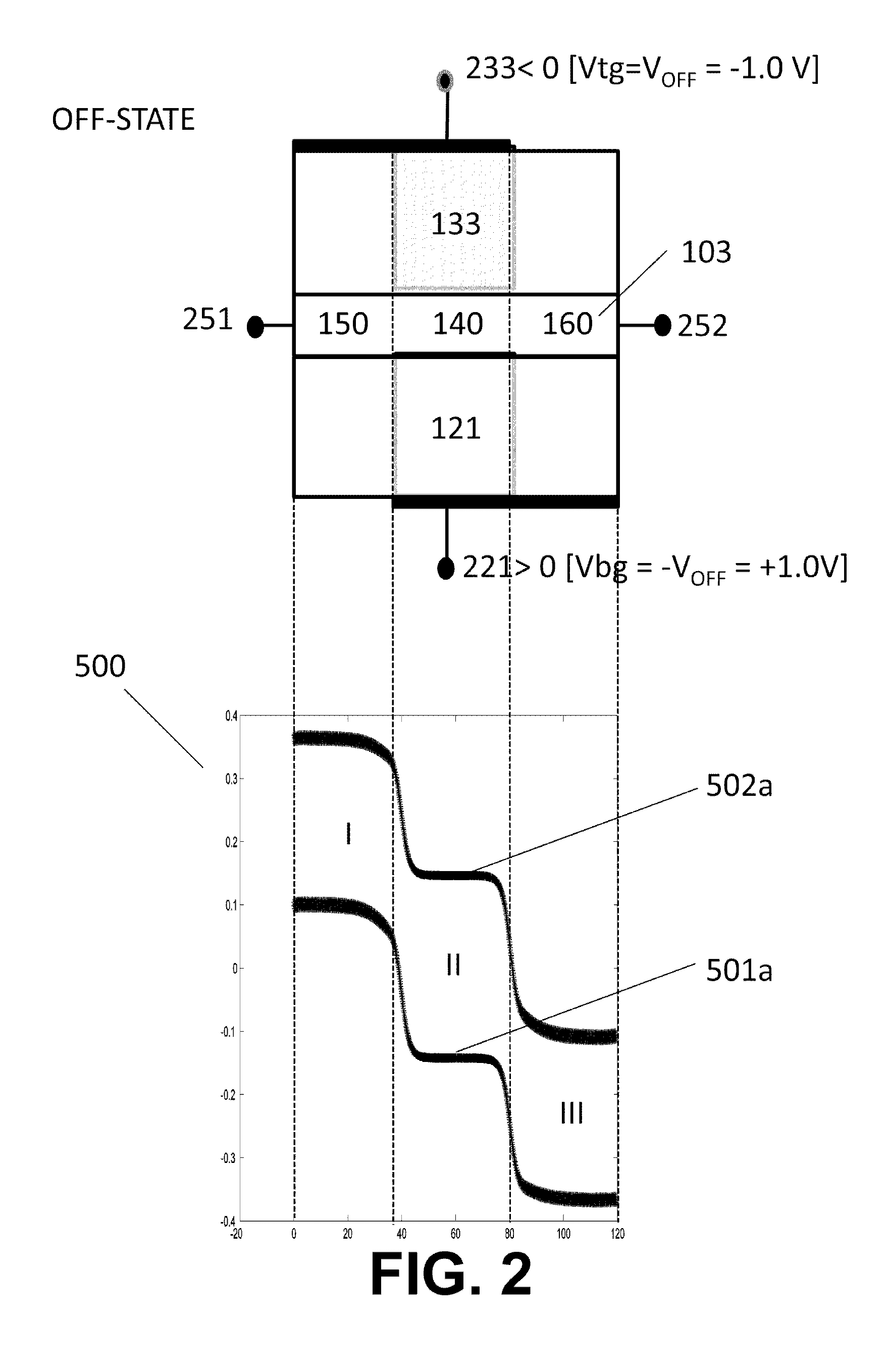
A bilayer graphene tunnelling field effect transistor is provided comprising a bilayer graphene layer, and at least a top gate electrode and a bottom gate electrode, wherein the at least a top gate electrode and a bottom electrode are appropriately positioned relative to one another so that the following regions are electrically induced in the chemically undoped bilayer graphene layer upon appropriate biasing of the gate electrodes: a source region, a channel region, and a drain region.

Description

INCORPORATION BY REFERENCE TO RELATED APPLICATIONS[0001]Any and all priority claims identified in the Application Data Sheet, or any correction thereto, are hereby incorporated by reference under 37 CFR 1.57. This application claims the benefit of EP Appl. No. 13197942.9 filed Dec. 18, 2013 and EP Appl. No. 14154114.4 filed Feb. 6, 2014. Each of the aforementioned applications is incorporated by reference herein in its entirety, and each is hereby expressly made a part of this specification.TECHNICAL FIELD[0002]The present disclosure relates to semiconductor devices comprising bilayer graphene (BLG) as well as to methods for the manufacturing and operating of such bilayer graphene (BLG) semiconductor devices.BACKGROUND OF THE DISCLOSURE[0003]Graphene is a 2-dimensional, semi-metallic, atomically-thin film in which carbon atoms are arranged into a sp2 honeycomb lattice structurally relying on in-plane, covalent σ-bonds. It is also chemically stable in non-oxidizing environments, and ...

Claims


Application Information

Patent Timeline
IPC IPC(8): H01L29/16
CPCH01L29/1606H01L29/42384H01L29/78648H01L29/78684H01L29/78696
Inventor NOURBAKHSH, AMIRHASANSOREE, BARTHEYNS, MARCAGARWAL, TARUN KUMAR
Owner INTERUNIVERSITAIR MICRO ELECTRONICS CENT (IMEC VZW)
Learn More