Eureka AIR delivers breakthrough ideas for toughest innovation challenges, trusted by R&D personnel around the world.

Method for producing a mechanically autonomous microelectronic device

Active Publication Date: 2015-06-04
COMMISSARIAT A LENERGIE ATOMIQUE ET AUX ENERGIES ALTERNATIVES
View PDF36 Cites 5 Cited by
  • Summary
  • Abstract
  • Description
  • Claims
  • Application Information

AI Technical Summary

Benefits of technology

The present invention allows for creating a microelectronic device with a stable and independent electric via. The method reduces defects in the interposers, such as breaking and bending, making them more durable.

Problems solved by technology

It must face many challenges, and more particularly the complex design, the problems entailed in thermal dissipation, the absence of standardisation, reliability, the definition of test strategies adapted to stacked circuits.
However, a certain number of drawbacks makes the use thereof difficult.
As a matter of fact, the current interposers are not mechanically stable because of their low thickness.
Even with an improved form factor, the length of the electric vias however requires the production and the utilisation of a very thin interposer, consequently having an inherent mechanical brittleness.
As silicon interposers have a major drawback in that they are relatively thin and thus mechanically fragile, electric measurements and tests are more and more difficult and may become soon almost impossible.
Interposers will probably be tested prior to assembling, and the cost of non-compliance will thus be very high.
Few companies are still capable of manufacturing both chips and interposers today.
But as they do not know how to perform testing and quantifying, it is very difficult for two distinct manufacturing companies to agree on non-compliance terms and conditions.
This means that a company producing chips and another company producing substrates will non longer cooperate, which will unavoidably affect the production lines of the companies not having a manufacturing unit, as well as the development costs.
The manufacturing process of a silicon interposer is currently difficult (and thus costly).
One of the main reasons (in addition to high costs) is that the current method requires the handling and processing of very thin wafers.
Bonding, and unbonding, which are followed by the handling of very thin components, thus become very difficult.
Generally speaking, the industry however was unable to agree on a reference technique; each technique has drawbacks.
Whatever the integration method selected for manufacturing silicon interposers, the final device is very thin.
This is the main technical challenge when designing interposers today, before cost.

Method used


Image

  • Method for producing a mechanically autonomous microelectronic device
  • Method for producing a mechanically autonomous microelectronic device
  • Method for producing a mechanically autonomous microelectronic device

Examples


Embodiment Construction

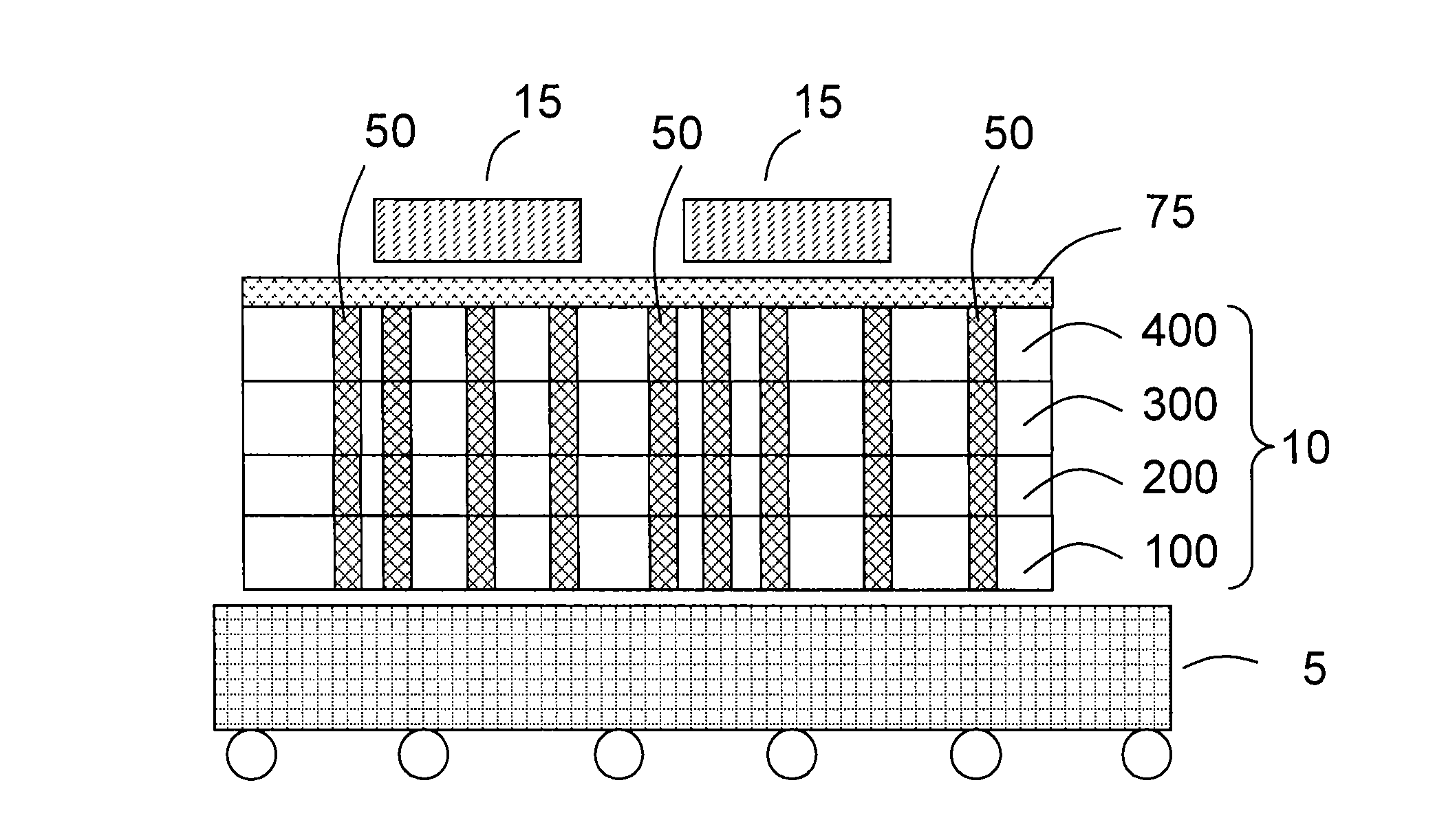
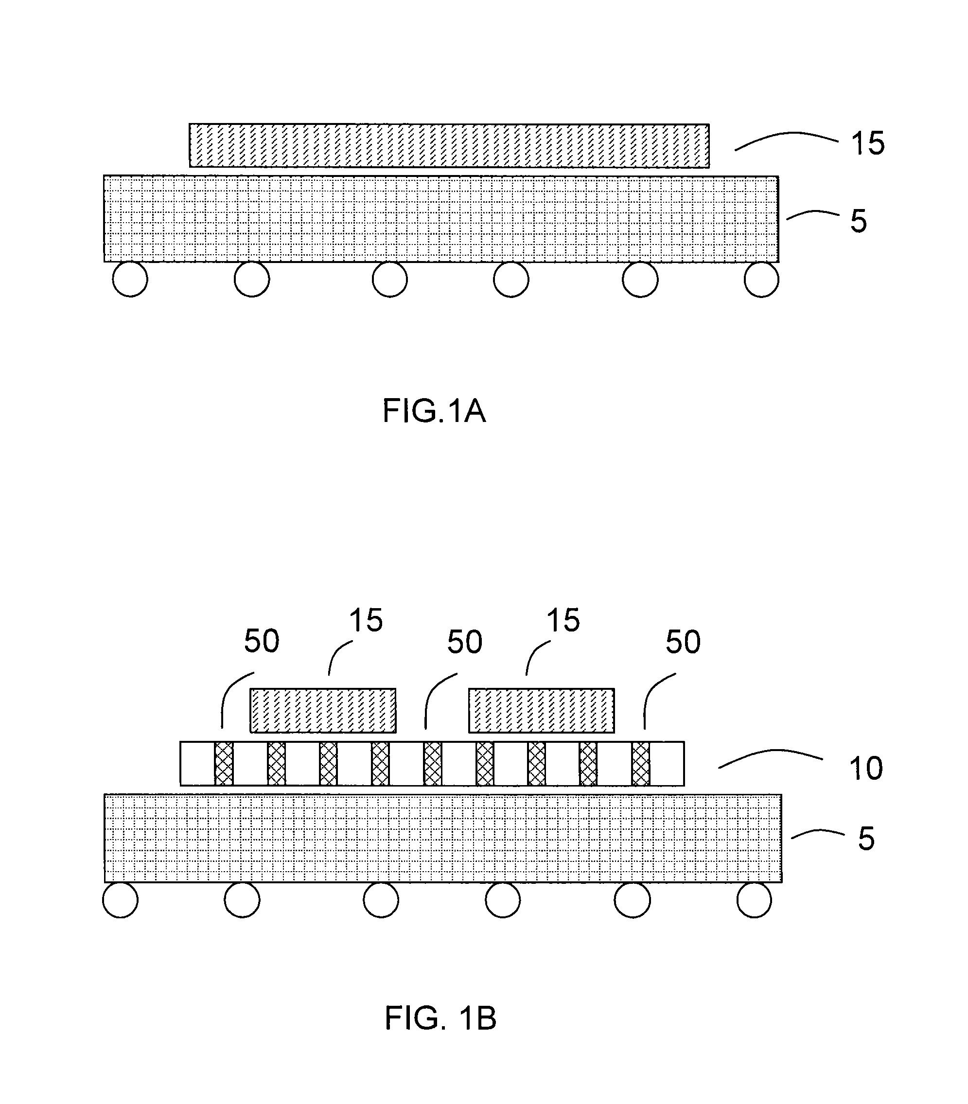
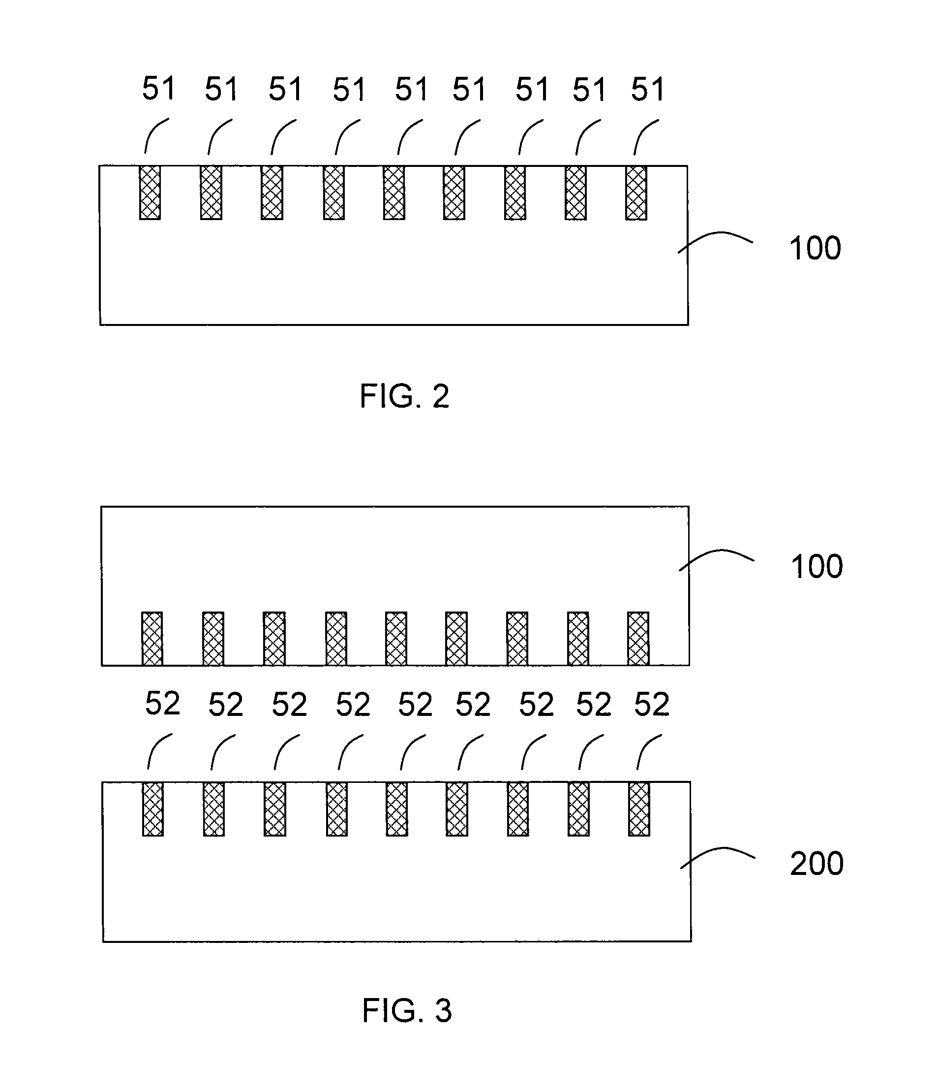
[0029]Before making a detailed review of the embodiments of the invention, optional characteristics which may be used in any combination or as alternative solutions are listed hereafter:[0030]The method comprises a step of assembling, including a direct bonding.[0031]The method comprises step of partially removing a part of the second substrate from a second face of the second substrate, opposite the first face of said second substrate, so as to reach the second portion of the electric via.[0032]The method comprises the production of at least another electric via simultaneously with said at least one electric via, with the vias comprising a material with thermal and electric properties so that said other electric via forms a thermal via.[0033]The method comprises a step of assembling at least another substrate on the first substrate and / or the second substrate.[0034]The method comprises a step of assembling comprising a step of aligning the first portion of the electric via of the f...


PUM

PropertyMeasurementUnit
Diameteraaaaaaaaaa
Diameteraaaaaaaaaa
Heightaaaaaaaaaa

Abstract

The invention relates to a method for producing a mechanically autonomous microelectronic device comprising at least one electric via enabling an electric connection from at least one first face of the device, characterized in that it comprises the following sequence of operations:from a first substrate comprising a first portion of the electric via exposed to a first face of the first substrate, and from a second substrate comprising a second portion of the electric via exposed to a first face of the second substrate, a step of bonding of the first substrate onto the second substrate, by bonding the first faces thereof so that the first portion and the second portion of the electric via are in electrical continuity,step of partially removing a part of the first substrate from a second face of the first substrate, opposite the first face of said first substrate, so as to reach the first portion of the electric via.

Description

FIELD OF THE INVENTION[0001]The present invention relates to 3D (three-dimension) integration, and more particularly 2.5D integration, also known as interposers technology. The invention more particularly relates to the production of a mechanically autonomous microelectronic device comprising at least one electric via.TECHNOLOGICAL BACKGROUND[0002]Referring to the Moore law which empirically foresees the doubling of integration of the components in the electronic industry every two years, the current developments of electronics are often mentioned as following two complementary directions . One development consists of More Moore miniaturisation , i.e. continually reducing the dimensions of the elementary components. Simultaneously, the More than Moore diversification defines the trend consisting in integrating more and more different functionalities in the same chip, whatever the degree of miniaturisation. Both developments are simultaneous and concern a wide range of technologies a...

Claims


Application Information

Patent Timeline
IPC IPC(8): H05K1/02H05K3/36H05K1/11
CPCH05K1/0206H05K3/36H05K1/0298H05K1/115H01L21/486H01L23/49827H01L23/49833H01L2924/0002H05K1/141H05K2201/10378Y10T29/49126
Inventor SCANNEL, MARK
Owner COMMISSARIAT A LENERGIE ATOMIQUE ET AUX ENERGIES ALTERNATIVES
Why Eureka
Eureka Blog
Learn More