
method to etch cu/ta/tan selectively using dilute aqueous hf/h2so4 solution

a technology of etching and solution, applied in the direction of solid-state devices, basic electric elements, semiconductor devices, etc., can solve the problems of reducing operational reliability, deteriorating leakage current characteristics, and device performance degradation, so as to prevent further etching and reduce potential copper diffusion damage

Inactive Publication Date: 2015-05-14
INTERMOLECULAR +1
View PDF4 Cites 12 Cited by
  • Summary
  • Abstract
  • Description
  • Claims
  • Application Information

AI Technical Summary

Benefits of technology

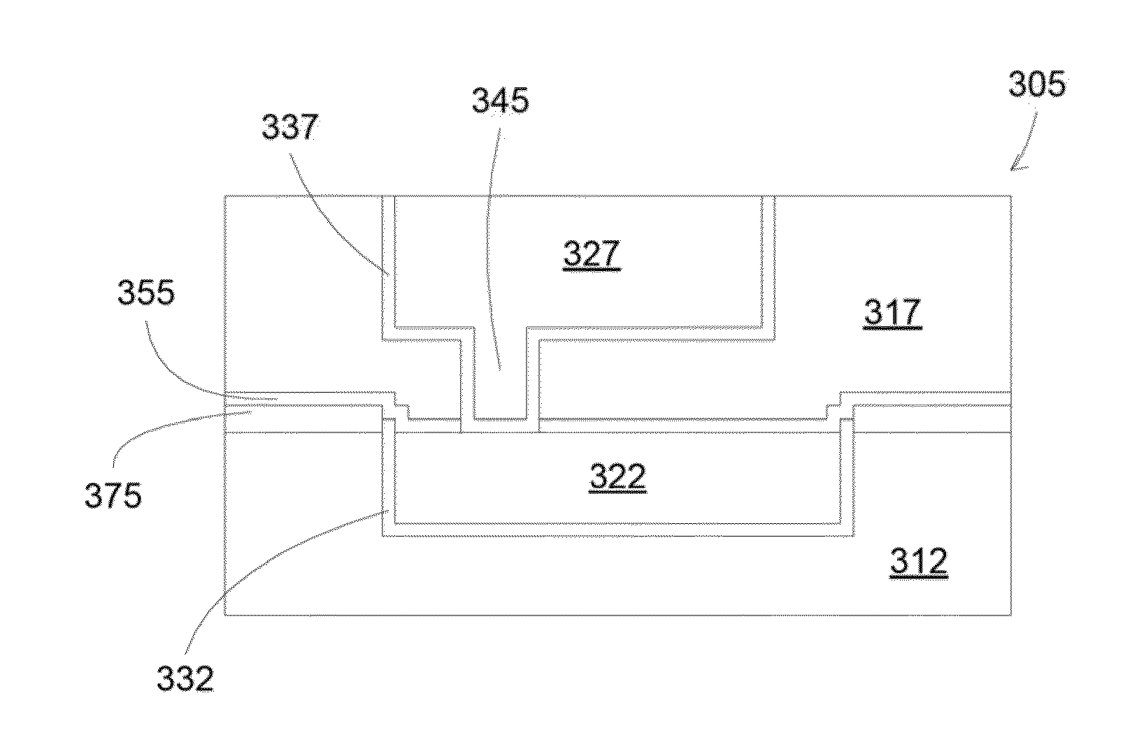
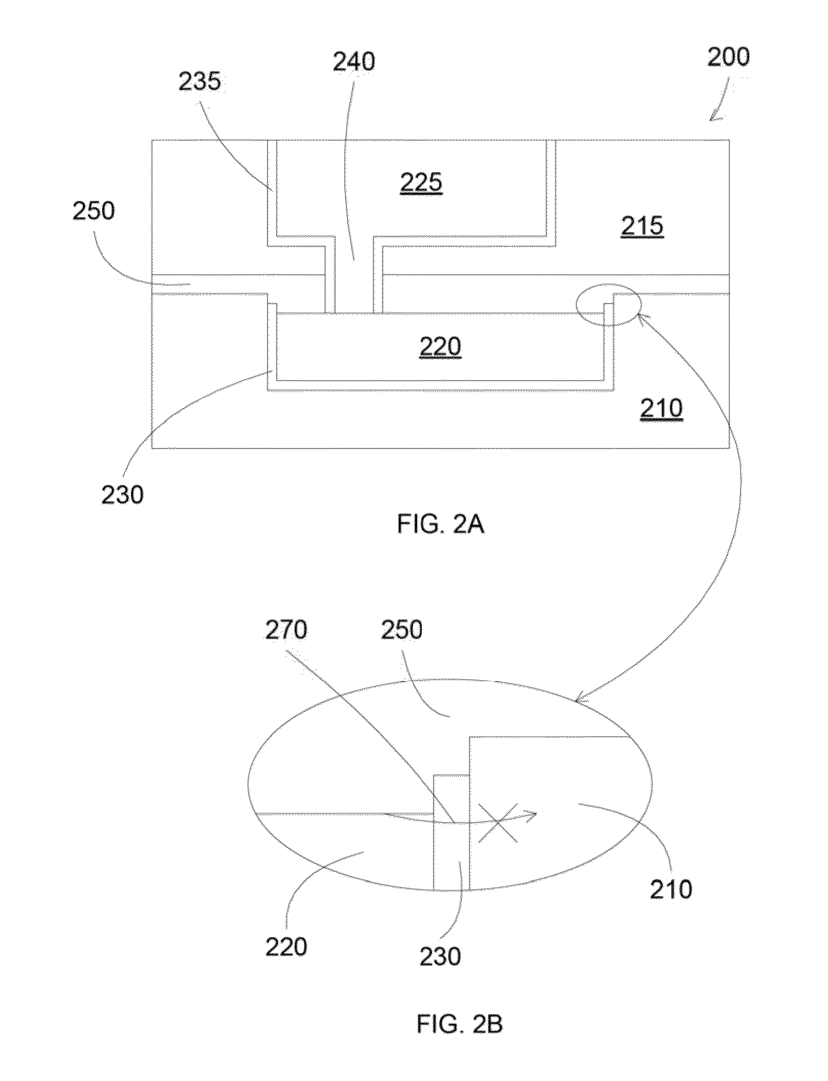
The patent describes methods for selectively etching copper while preserving a protective liner in semiconductor devices. This helps to prevent copper contamination and reduces potential damage to the device. The process involves recessing the copper film deeper than the liner film to enhance protection. The liner film can be recessed between 1.5 and 2 nm, while the copper film can be recessed between 2 and 3 nm. The recessing process can be performed with a wet etch process for between 30 and 60 seconds at a temperature between 25 and 40 C. A water rinse can be performed to remove the etch solution and further etching can be prevented. Additionally, a SiC layer can be formed on the dielectric layer to protect it during the recess process and reduce copper diffusion damage.

Problems solved by technology

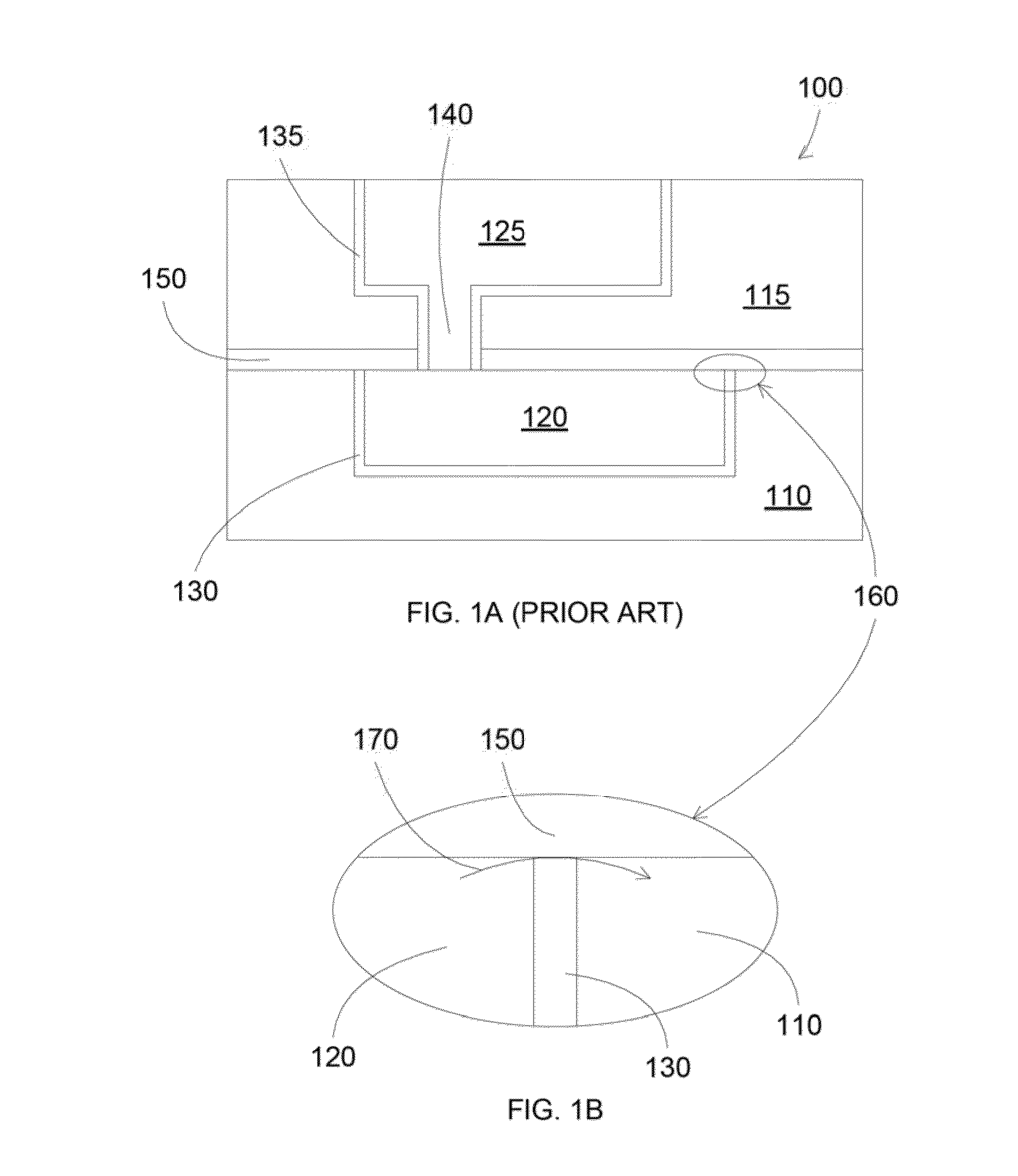
For example, copper can diffuse into the surrounding dielectric materials at low temperatures, leading to device performance degradation.
For example, after the planarization, copper can migrate over time to cause bridges between adjoining copper wirings, leading to the deterioration of leakage current characteristics.
The weak spots thus can decrease operational reliability due to current leakage and thus increase the risk of operational breakdown, such as time dependent dielectric breakdown (TDDB).
In addition, high electric field can be observed at the top edges of the interconnect lines, which can cause operational breakdown or electromigration failures due to the high electrical field concentration.

Method used


Image

  • method to etch cu/ta/tan selectively using dilute aqueous hf/h2so4 solution
  • method to etch cu/ta/tan selectively using dilute aqueous hf/h2so4 solution
  • method to etch cu/ta/tan selectively using dilute aqueous hf/h2so4 solution

Examples


Embodiment Construction

[0025]A detailed description of one or more embodiments is provided below along with accompanying figures. The detailed description is provided in connection with such embodiments, but is not limited to any particular example. The scope is limited only by the claims and numerous alternatives, modifications, and equivalents are encompassed. Numerous specific details are set forth in the following description in order to provide a thorough understanding. These details are provided for the purpose of example and the described techniques may be practiced according to the claims without some or all of these specific details. For the purpose of clarity, technical material that is known in the technical fields related to the embodiments has not been described in detail to avoid unnecessarily obscuring the description.

[0026]In some embodiments, methods are provided to form copper interconnect structures having improved reliability. For example, copper and barrier liner can be recessed with ...


PUM

PropertyMeasurementUnit
timeaaaaaaaaaa
timeaaaaaaaaaa
timeaaaaaaaaaa

Abstract

Copper can be etched with selectivity to Ta / TaN barrier liner and SiC hardmask layers, for example, to reduce the potential copper contamination. The copper film can be recessed more than the liner to further enhance the protection. Wet etch solutions including a mixture of HF and H2SO4 can be used for selective etching copper with respect to the liner material, for example, the copper film can be recessed between 2 and 3 nm, and the barrier liner film can be recessed between 1.5 and 2 nm.

Description

FIELD OF THE INVENTION[0001]The present invention relates generally to methods for fabricating an integrated-circuit device, and particularly to selective wet etches processes between copper, tantalum and tantalum nitride.BACKGROUND OF THE INVENTION[0002]Current technologies for fabricating ultra-large scale integrated-circuit devices employ copper interconnects. Interconnections using copper have replaced aluminum in the fabrication of ultra-large scale integrated-circuit devices due to its lower specific resistance and improved electromigration (EM) characteristics.[0003]Usually, the copper interconnects are surrounded by barrier liners, such as tantalum (Ta) and / or tantalum nitride (TaN), to prevent outdiffusion and corrosion of the copper interconnect lines. For example, copper can diffuse into the surrounding dielectric materials at low temperatures, leading to device performance degradation. Copper can also be oxidized and corroded during the standard processing of device fabr...

Claims


Application Information

Patent Timeline
Patent Type & Authority Applications(United States)
IPC IPC(8): H01L23/522H01L23/532
CPCH01L23/5228H01L23/5226H01L23/5329H01L23/53261H01L23/53257H01L23/53238H01L23/53295H01L21/32134C23F1/02C23F1/18C23F1/26H01L2924/0002H01L21/76883H01L21/76834H01L2924/00
Inventor DUONG, ANHRYAN, ERROL TODD
Owner INTERMOLECULAR
Learn More