CMOS image sensor system and method thereof

a technology of image sensor and image sensor, which is applied in the field of image sensor system, can solve the problems of affecting the image quality of the image produced by the method cannot be applied to the cmos image sensor made using conventional process and packaging, and the image quality of the cmos image sensor is not as good as that of the ccd image sensor, so as to prevent dc voltage variations and noise interference from affecting the image quality, avoid dc voltage variations and noise interferen

Inactive Publication Date: 2015-04-02
UCHANGE TECH
View PDF3 Cites 0 Cited by
  • Summary
  • Abstract
  • Description
  • Claims
  • Application Information

AI Technical Summary

Benefits of technology

[0009]The disclosed method includes the steps of: generating a controlling signal to make a input terminal repeatedly switch between high and low potentials; after detecting light and generating charges, generating DC and AC signals according to the high / low potential on the input terminal, and outputting the DC and AC signals to the column output; filtering out the DC signal from the column output and receiving only the AC signal to avoid DC voltage variations and noise interference, and processing the AC signal to generate an image signal.
[0010]The disclosed system and method differ from the prior art in that the controlling signal is produced to switch the input terminal between the high and low potentials, thereby modulating the image signal at a specific frequency to prevent DC voltage variations and noise interference from affecting the image quality.

Problems solved by technology

Generally speaking, the quality of images produced by a CMOS image sensor is not as good as that by a CCD image sensor.
It is thus the primary issue for vendors to improve the image quality of CMOS.
However, this method cannot be applied to the CMOS image sensor made using conventional process and packaging.
On the other hand, new manufacturing processes and structures result in lower yield and higher cost.
Therefore, the above-mentioned solution cannot effectively address the problem of bad image quality for CMOS.
In summary, the prior art always has the problem of bad image quality for CMOS image sensors.

Method used


Image

  • CMOS image sensor system and method thereof
  • CMOS image sensor system and method thereof
  • CMOS image sensor system and method thereof

Examples


Embodiment Construction

[0018]The present invention will be apparent from the following detailed description, which proceeds with reference to the accompanying drawings, wherein the same references relate to the same elements.

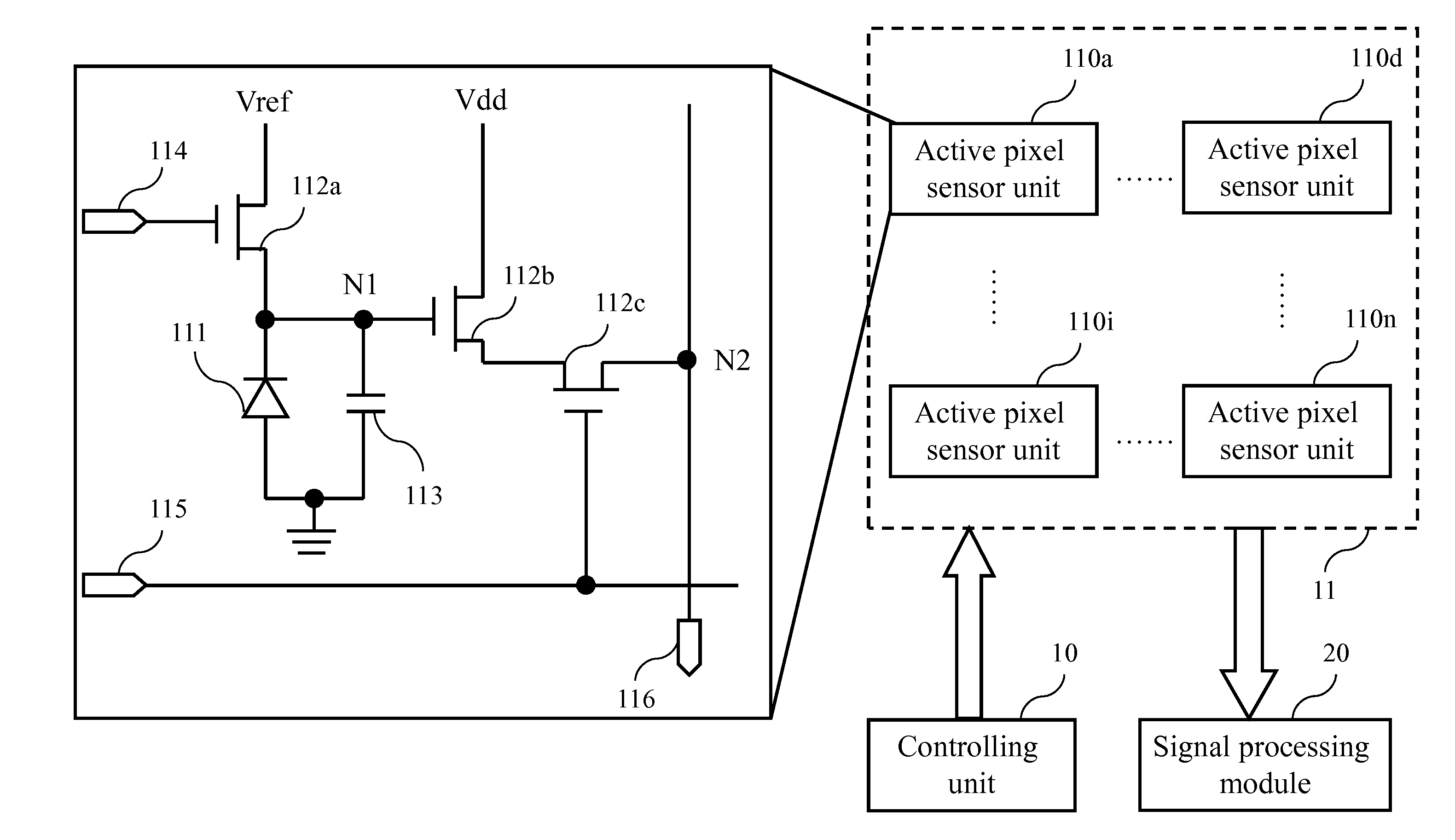
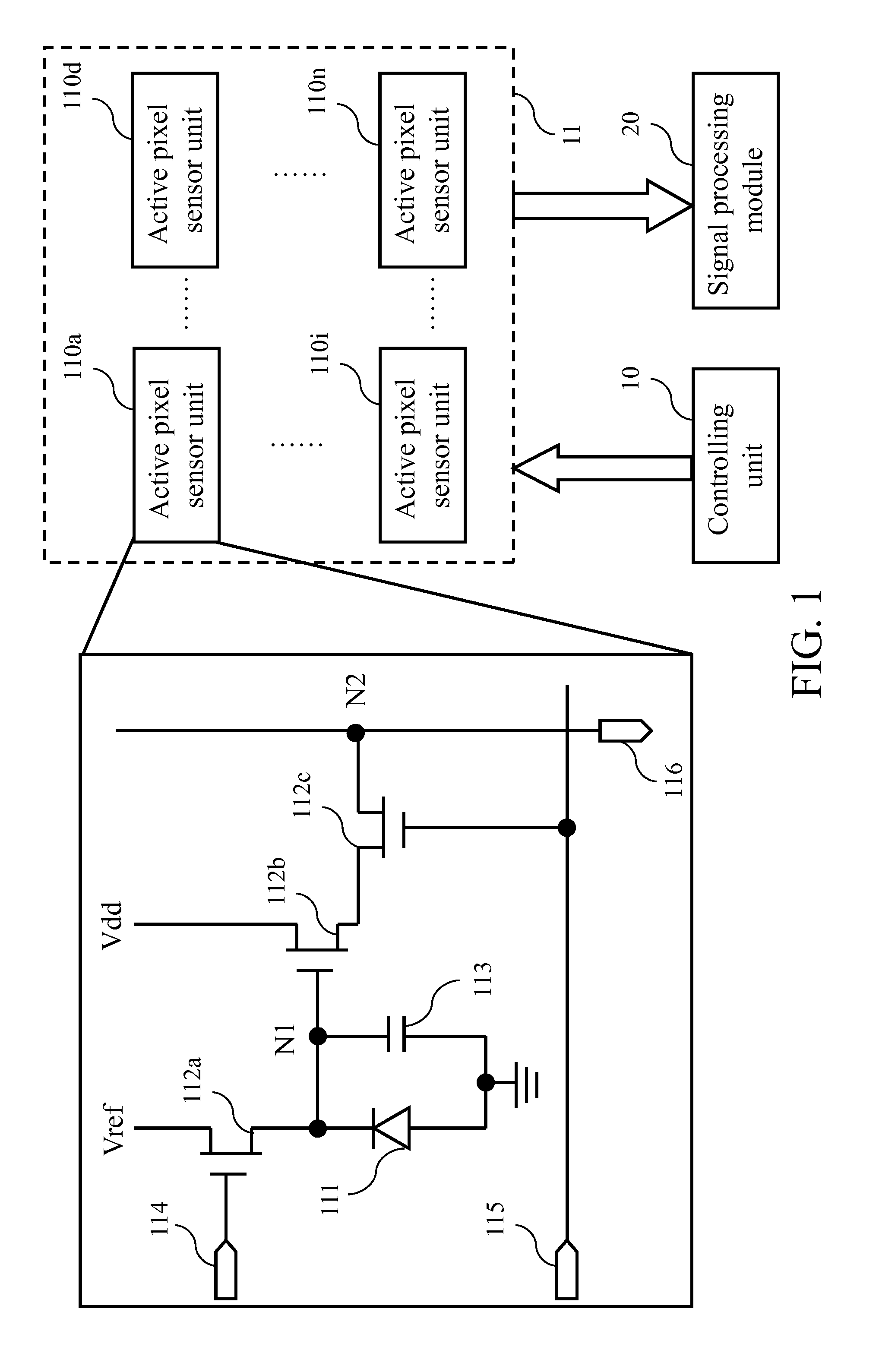
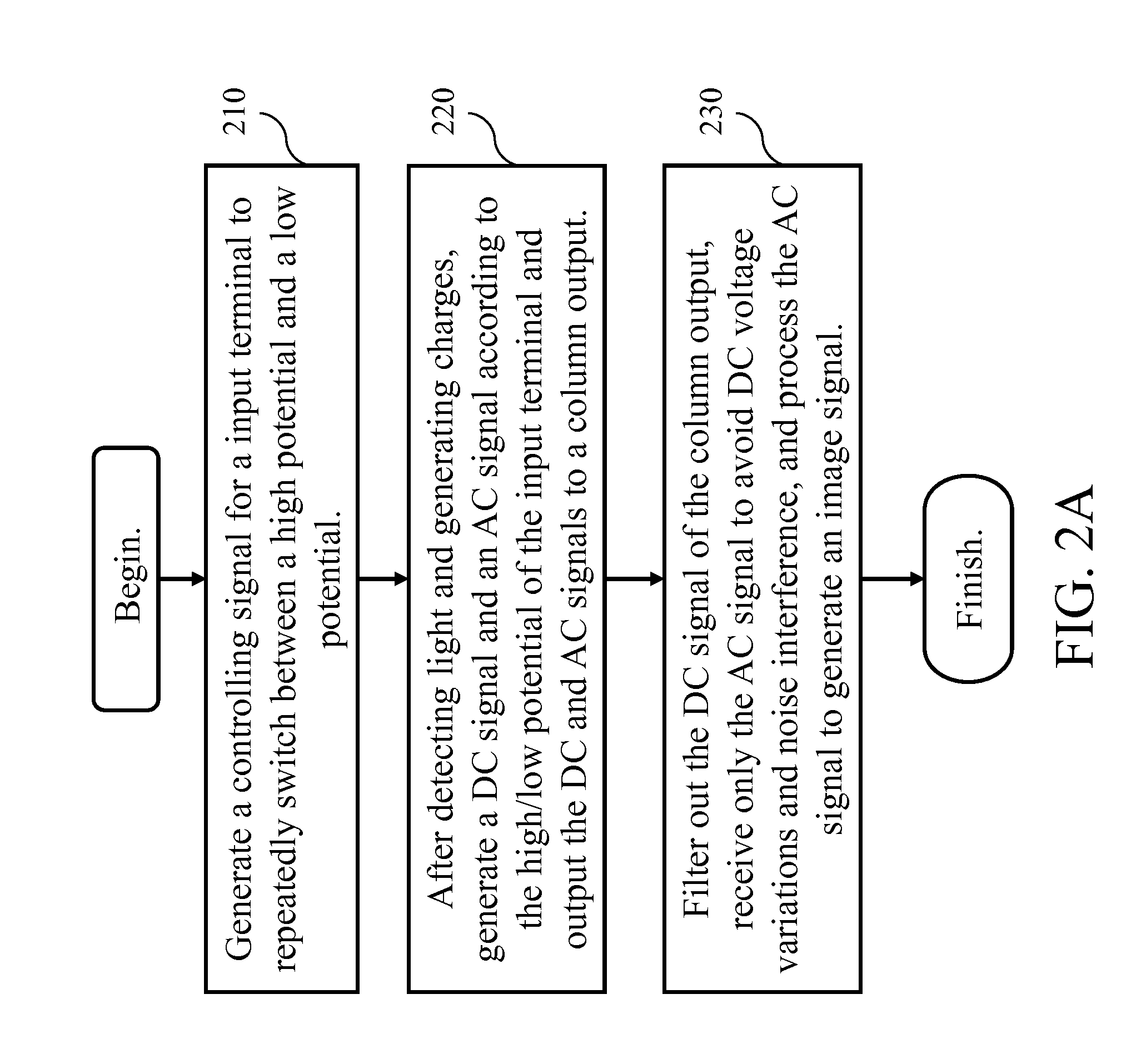
[0019]Before describing the disclosed CMOS image sensor and the method thereof in detail, we first explain the structure of the invention. The invention differs from the prior art in that in the active pixel sensor unit, the input terminal repeatedly switches between high and low potentials to obtain DC and AC signals. The DC signal is then filtered out, leaving the AC signal to be detected and used for image formation. In comparison, the prior art can only obtain and use the DC signal. Thus, the invention can prevent DC signal shifts due to differences in electronic properties, thereby avoiding bad image quality. The invention can be applied to a conventional sensor array and achieve the goal of image quality improvement. Besides, semiconductors have higher flicker noises on low-freq...


PUM


Abstract

A complementary metal-oxide semiconductor (CMOS) image sensor system and method thereof produce a control signal to make a input terminal repeatedly switch between high potential and low potential, thereby modulating image signals at a specific frequency to prevent image quality from being affected by direct current (DC) voltage variations. The mechanism thus helps improving the image quality.

Description

CROSS-REFERENCE TO RELATED APPLICATION[0001]This application claims priority to TAIWAN Patent Application Ser. No. 102127073, filed Jul. 29, 2013, the entireties of which is incorporated herein by reference.TECHNICAL FIELD[0002]The invention relates to an image sensor system and, in particular, to a CMOS image sensor system that utilizes CMOS as an active pixel image sensor. The invention also relates to the method thereof.BACKGROUND ARTDescription of Related Art[0003]In recent years, rapid developments and popularity of semiconductor technology have enabled complementary metal-oxide semiconductor (CMOS) image sensors to compete with charge coupled device (CCD) sensors. Particularly in the low-end market, the CMOS image sensors have a lower cost because they do not require a special manufacturing process. Therefore, the CMOS image sensors have become the mainstream in the low-end market.[0004]Generally speaking, the quality of images produced by a CMOS image sensor is not as good as...

Claims


Application Information

Patent Timeline
Patent Type & Authority Applications(United States)
IPC IPC(8): H04N5/357H04N5/374
CPCH04N5/374H04N5/357H04N25/60H04N25/76H04N25/75
Inventor CHANG, CHIH-TSUNGSIE, JYUN-JIE
Owner UCHANGE TECH
Why Eureka
Try Eureka