Eureka AIR delivers breakthrough ideas for toughest innovation challenges, trusted by R&D personnel around the world.

Display panel with agglomerates

a technology of agglomerates and display panels, applied in the field of display panels, can solve the problems of light leakage in the dark state around the spacers of conventional display panels, and achieve the effect of improving light leakag

Active Publication Date: 2015-03-19
INNOLUX CORP
View PDF1 Cites 5 Cited by
  • Summary
  • Abstract
  • Description
  • Claims
  • Application Information

AI Technical Summary

Benefits of technology

This invention is about a display panel that reduces the amount of light leakage around the edges of the panels. This is accomplished by adding "agglomerates" around the spacers in the panel. This improves the dark state of the panel by preventing light from leaking through the space between the two substrates. The panel also includes an orientation patterned polymer layer that helps improve image quality by smoothing the surface of the display.

Problems solved by technology

However, the defect of light leakage in the dark state occurs around the spacers of a conventional display panel, due to the liquid crystal molecules adjacent to the spacers are tilted along the surface of the spacers.

Method used


Image

  • Display panel with agglomerates
  • Display panel with agglomerates
  • Display panel with agglomerates

Examples


first embodiment

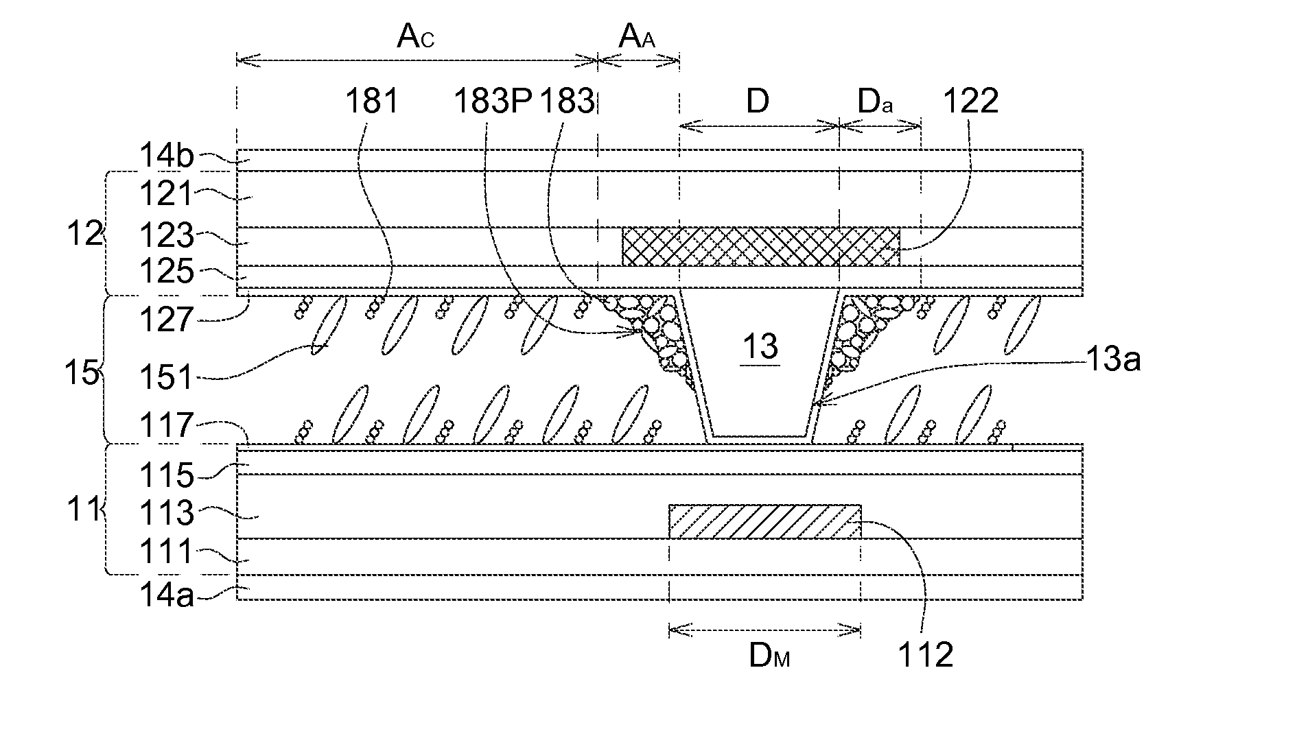
[0024]As shown in FIG. 1A, the second substrate 12 of an embodiment comprises a second base 121, a second transparent conductive layer 125 and a second alignment film 127 formed on the second transparent conductive layer 125. Material such as polyimide (PI) can be used for fabricating the second alignment film 127. The second transparent conductive layer 125 can be an ITO layer. The second substrate 12 further comprises a light-shielding patterned layer 122 (for example, the black matrix, BM) and a color filter photoresist layer 123 formed on the second base 121. the second substrate 12 further comprises a plurality of spacers 13 formed on the second transparent conductive layer 125, and the second alignment film 127 contacts and covers the spacers 13. Setting the spaces 13 maintains a uniform gap (i.e. cell gap) between the first substrate 11 and the second substrate 12, and liquid crystal material is filled in the gap to form the liquid crystal layer 15.

[0025]Furthermore, a first...

second embodiment

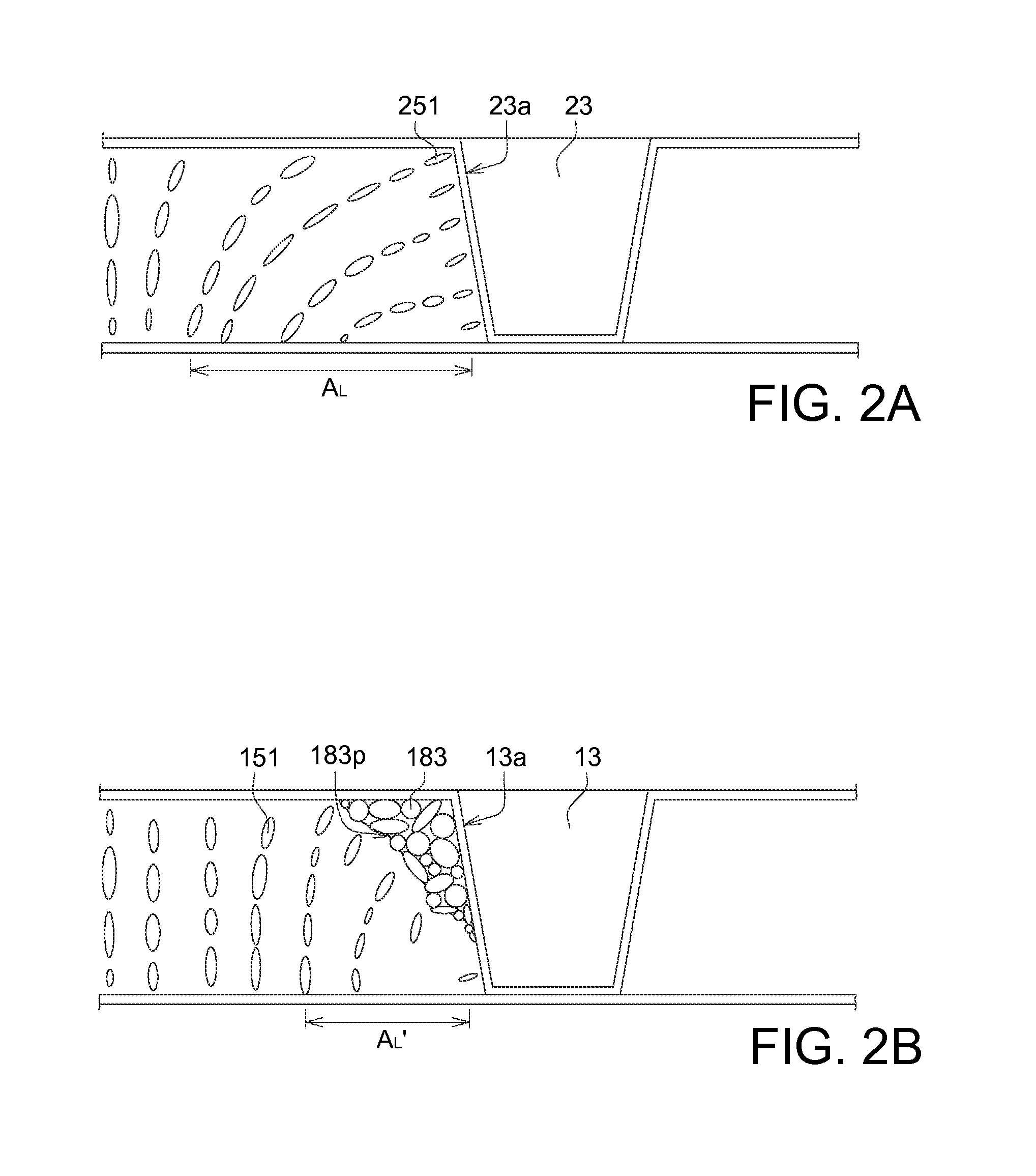
[0039]In the second embodiment, the second transparent conductive layer 425 has a plurality of openings respectively formed between two of the spacers 43. As shown in FIG. 4, the openings 49a and 49b are disposed adjacent to the spacer 43 to facilitate control of the electrical field near the spacer 43 during the polymerization, thereby inducing a disorder polymerization around the spacer 43. After the monomers are subjected to the UV-light irradiation under the control of the electrical field, the orientation regions AC comprising the polymer chains 481 and the agglomeration regions AA comprising polymer agglomerates 483 are formed consequently. The polymer agglomerates 483 surround the spacer 43. The distribution profile 483P constituted by the polymer agglomerates 483 is slanted to the surface of the spacer 43, for pressing and leading the LC molecules near the spacer 43 to a more vertical alignment. Therefore, the region of light leakage adjacent to the spacer 43 is capable of b...


PUM

PropertyMeasurementUnit
sizesaaaaaaaaaa
sizeaaaaaaaaaa
Daaaaaaaaaaa

Abstract

A display panel comprises a first substrate having a first alignment film, a second substrate having a second alignment film and plural spacers, a liquid crystal layer disposed between the first and second substrates, and a plurality of agglomerates positioned between the first and second alignment films and further surrounding at least one of the spacers. The spaces maintain a uniform gap between the first and second substrates. The second alignment film is disposed oppositely to the first alignment film and covers the spacers. In one embodiment, sizes of the agglomerates are distributed in a range of 0.1 μm˜2 μm.

Description

[0001]This application claims the benefit of Taiwan application Serial No. 102133495, filed Sep. 16, 2013, the subject matter of which is incorporated herein by reference.BACKGROUND[0002]1. Field of the Invention[0003]The disclosure relates in general to a display panel, and more particularly to a display panel with agglomerates.[0004]2. Description of the Related Art[0005]Today, electronic products with displays, such as smart phones, tablet personal computers (i.e. tablet PC, flat PC, ex: iPad), laptops, monitors, and televisions, are necessary tools for work and leisure in the daily life. Liquid crystal display (LCD) is the most popular displays in use. Being compact in size, light in weight, power-saving and radiation-free, LCDs are the most popular displays in use.[0006]LCD is a flat panel display, electronic visual display, or video display that uses the light modulating properties of liquid crystals. LCD possesses the excellent characteristics such as compact in size, light w...

Claims


Application Information

Patent Timeline
Patent Type & Authority Applications(United States)
IPC IPC(8): G02F1/1339G02F1/1335G02F1/1343G02F1/1362G02F1/1337
CPCG02F1/13394G02F1/1362G02F1/1337G02F2001/13398G02F1/133512G02F1/133514G02F1/133528G02F1/13439G02F1/133711G02F1/133776G02F1/13398
Inventor CHEN, CHENG-HSIUNGYEH, YU-LINWANG, AN-CHANGCHEN, YI-CHING
Owner INNOLUX CORP
Why Eureka
Eureka Blog
Learn More