
Process module, fabricating method thereof and substrate processing method using the process module

Inactive Publication Date: 2015-02-26
KWAK JAE JEONG +1
View PDF1 Cites 6 Cited by
  • Summary
  • Abstract
  • Description
  • Claims
  • Application Information

AI Technical Summary

Benefits of technology

The substrate processing method using a process module according to the present invention offers several technical effects: high productivity, price competitiveness, and minimization of substrate damage even under circumstance of separate substrate processing processes. It is particularly advantageous for fabricating substrates used in display devices such as smartphones due to its lateral strength maintenance process. It can also be applied to processing of cell substrates that are difficult to adjust their final dimension, and it may increase productivity in the process of attaching devices to each other.

Problems solved by technology

However, in “the sheet method”, it is difficult to cut the surface-strengthened bare sheet into the unit of cells, and the strength of a cut surface, i.e., a side of the cell substrate is lowered due to micro cracks generated in cutting, so that product durability is reduced and yield is lowered due to the difficulty of mechanical machining.
But, since the cutting and polishing are performed basically with respect to the surface-strengthened bare sheet, it is difficult to machine a curved side or holes inside, so that an appearance design is limited.
And, although strengthening is performed as a post process, it is difficult to secure sufficient strength, thus causing durability problem, so that the cutting and polishing have a difficulty in application of mass production.
In spite of efforts for solving problems caused in the cutting in such a “sheet method”, since the “sheet method” may not give the sufficient strength to the side of substrate cut and exposed, the “sheet method” is limitedly applied only to the fabrication of substrates used in tablet PCs or display devices for notebook computers in which sufficient displaying area may be secured by covering the wide width of bezel with another structural element such as a case or a frame to augment the strength of the side.
Consequently, the “sheet method” has an inherent limitation in that it may be limitedly applied only to the fabrication of substrates requiring a low lateral strength among substrates used in display devices with a minimized bezel width.
But in case the chemical strengthening is adopted in the “sheet method”, since a printed layer or a thin film layer formed previously may be damaged by a high temperature chemical material, strengthening of the side of the cell substrate in the “sheet method” is practically impossible.
However, since, in the method disclosed in Korean Patent Application No. 10-2013-0011942, the size of the thickness partly cut should be a maximum in order to secure the lateral strength of a cut surface, this Korean Patent Application No. 10-2013-0011942 has a possibility that an uncut portion is inadvertently damaged during the substrate processing process in the unit of sheets.
As mentioned above, since the existing “sheet method” not only has advantages such as simplicity of process and high productivity, but also has inherent limitations in that the supplementation of the strength of a cut surface is not sufficient and strengthening is difficult, the “cell method” in which cell substrates is previously separated from a bare sheet to be polished and strengthened before a substrate processing process, is generally adopted as a practical solution for fabricating a substrate applicable to a display device, such as a smartphone with high portability and a minimized bezel width.
However, the “cell method” has also the problem such as lower productivity and price competitiveness than the “sheet method”, because the substrate processing process is performed in the state that each of the cell substrates is received in each of individual jigs in the “cell method”.
Further, the “cell method” has a practical problem in that the cutting process is performed prior to the substrate processing process.
That is, the current cutting technique has a tolerance in a range of ±30 μm due to technical limitations.
In particular, such substrate alignment and temporary fixing should be repeatedly performed before each of plural substrate processing processes, and thereby the low productivity in the “cell method” get further deteriorated.
As a result, not only the possibility each cell substrate itself may be directly exposed to an external environment to damage but also the incidental expense for preventing such a damage is increased at the same time.
As described above, in processing the window substrate used in a display device, such as the smartphone with high portability and a minimized bezel width, the existing “sheet method” has unsolved problems in that the processing quality of a cut surface and the lateral strength decrease, and the existing “cell method” has unsolved problems in that the productivity and the price competitiveness decrease.

Method used


Image

  • Process module, fabricating method thereof and substrate processing method using the process module
  • Process module, fabricating method thereof and substrate processing method using the process module
  • Process module, fabricating method thereof and substrate processing method using the process module

Examples


Embodiment Construction

[0104]Hereinafter, embodiments of the present invention will be described in detail with reference to the accompanying drawings. In drawings, the same elements or equivalents are referred to with the same or similar reference numerals.

[0105]When it is said that a part “includes” an element, it means that the part may further include other elements unless it is said that the part does not include other elements explicitly.

[0106]Also, when it is said that an element is “selectively” provided, equipped, or included, it means that the element is not an element essentially selected for solving an object of the present invention but may be arbitrarily selected with relation to the object to be solved.

(Overall Substrate Processing Method)

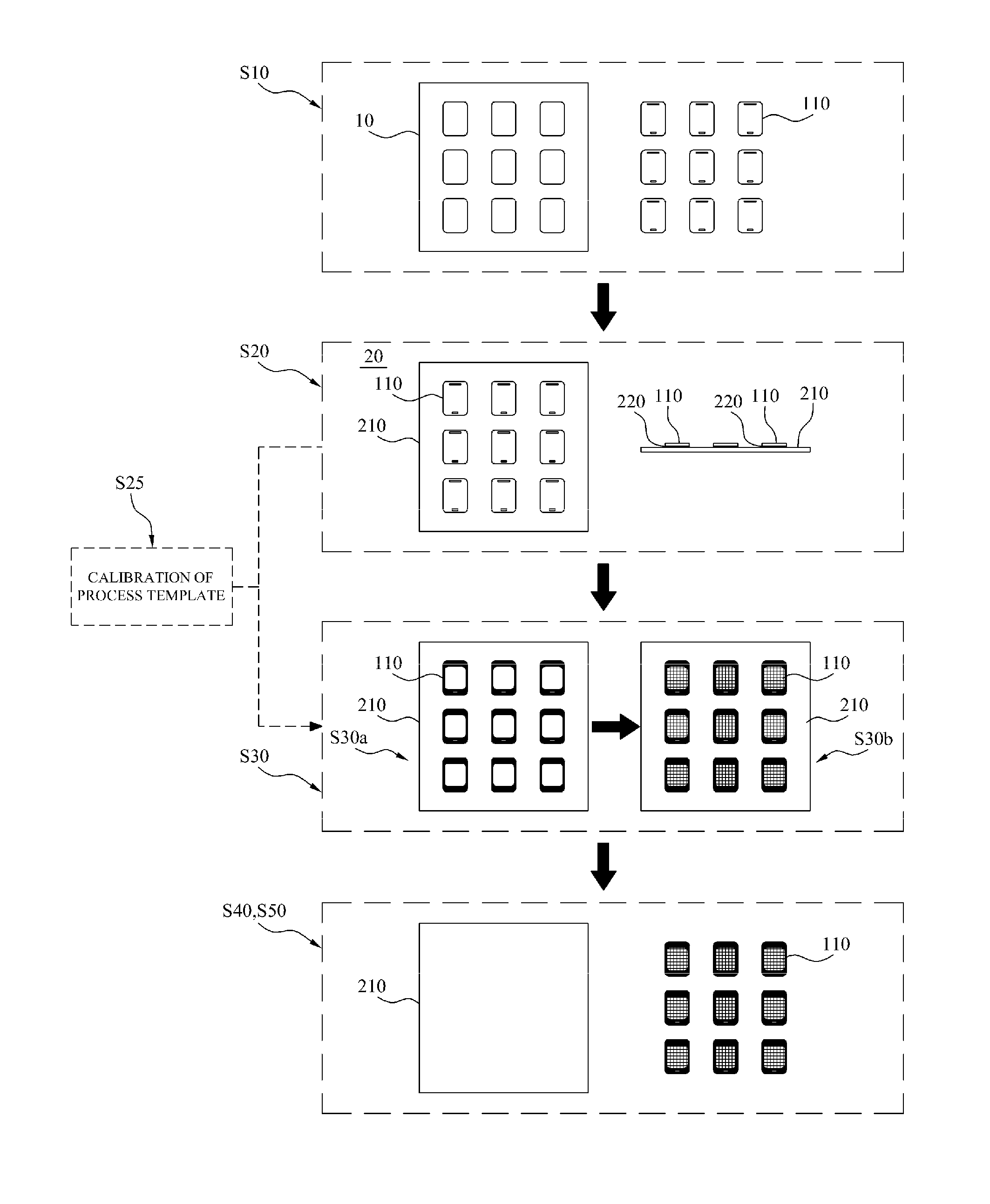
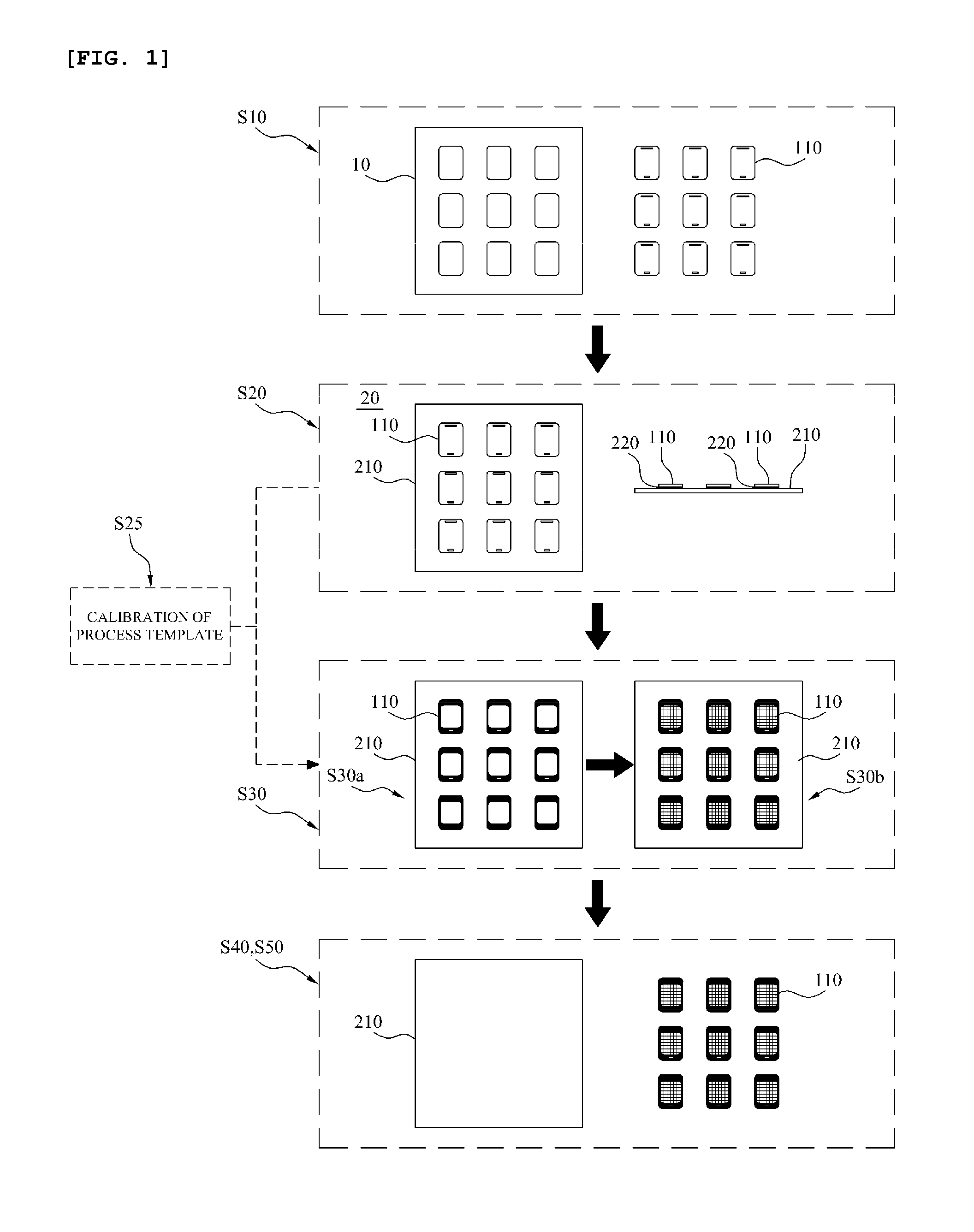
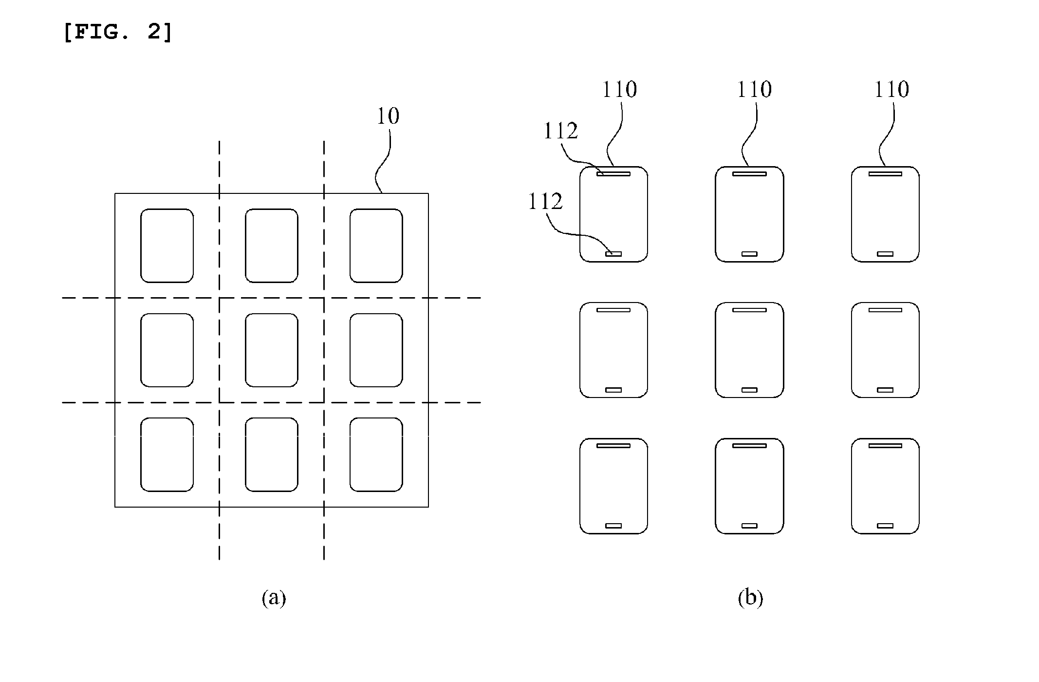
[0107]FIG. 1 is a schematic view illustrating a substrate processing method according to an embodiment of the present invention. The substrate processing method includes an operation (S10) of preparing a substrate including separating a plurality of cell s...


PUM

PropertyMeasurementUnit
Timeaaaaaaaaaa
Dimensionaaaaaaaaaa
Thermal expansion coefficientaaaaaaaaaa

Abstract

Disclosed are a process module, a fabrication method thereof, and a substrate processing method using the process module. The process module includes a structure in which cell substrates are fixed on a carrier member by an adhesive according to a preset alignment standard. The fabrication method includes aligning the cell substrates according to a preset alignment standard, applying an adhesive to at least one of surfaces facing each other between the cell substrates and the carrier member, and attaching the cell substrates to the carrier member by using the adhesive. The substrate processing method includes performing the substrate processing process of the cell substrates at the same time by using the process module integrated with the cell substrates. The substrate processing method selectively includes calibrating the alignment standard for the cell substrates in the substrate processing process to an alignment state of the cell substrates in the process module.

Description

TECHNICAL FIELD[0001]The present invention relates to a process module, a fabricating method thereof, and a processing method of a substrate using the process module.[0002]The term “substrate” used herein relates to a surface element used in a display device.[0003]Also, the term “processing” includes a process for providing a decorative element, such as a surface pattern, and a process for providing a functional element, such as a thin film, on a substrate.BACKGROUND ART[0004]For substrates recently used in display devices, surface-strengthened glass is adopted for a cover glass or a touch screen glass constituting the outer surface of the display device for protection from abrasion and impact. In particular, in the case of substrates used in display devices with high portability and minimized bezel width, for example, smartphones, since the sides of substrate are vulnerable to external impact, mechanical or chemical polishing is performed to reduce micro cracks and thus improve the...

Claims


Application Information

Patent Timeline
IPC IPC(8): B32B38/10B32B37/12
CPCB32B38/10B32B2457/20B32B37/1284B32B37/12B32B2457/208G06F2203/04103Y10T156/10Y10T156/17G06F3/0443
Inventor LIM, YONG JINKWAK, JAE JEONG
Owner KWAK JAE JEONG
Learn More