
Semiconductor device and method of manufacturing semiconductor device

Active Publication Date: 2015-01-22
FUJI ELECTRIC CO LTD
View PDF0 Cites 4 Cited by
  • Summary
  • Abstract
  • Description
  • Claims
  • Application Information

AI Technical Summary

Benefits of technology

The invention improves the precision of recognizing the position of an alignment marker on a semiconductor device by concentrating portions that scatter light in the alignment marker. Additionally, the invention highlights and brightens portions of the alignment marker that reflect light based on its concavities and convexities. The structure of the alignment marker is formed after the semiconductor device is micronized, and the process of exposing the concavities and convexities of the first metal film does not adversely affect the recognition precision of the alignment marker. The invention enables the formation of an alignment marker with high recognition precision while also allowing for micronization of the semiconductor device.

Problems solved by technology

In addition, since the sizes of the opening portion and the contact hole are small to be unrecognizable for an image recognition apparatus, the alignment marker can be recognized with high precision without using an expensive image recognition apparatus capable of recognizing fine patterns.
In other words, in a semiconductor device in which the alignment marker disclosed in U.S. Pat. No. 4,967,904 is disposed, there is a problem in that micronization is difficult to be achieved.

Method used


Image

  • Semiconductor device and method of manufacturing semiconductor device
  • Semiconductor device and method of manufacturing semiconductor device
  • Semiconductor device and method of manufacturing semiconductor device

Examples


embodiment 1

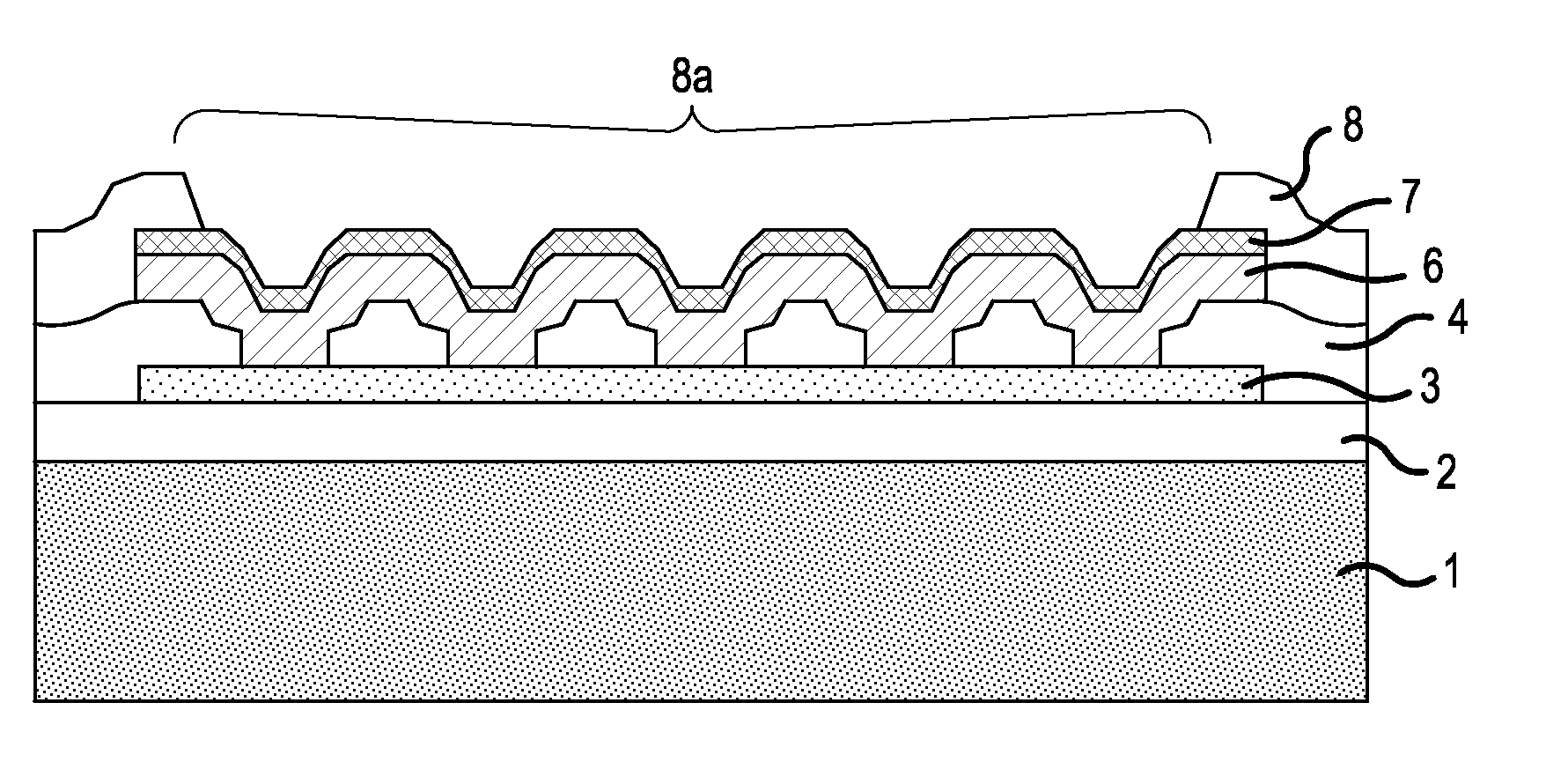
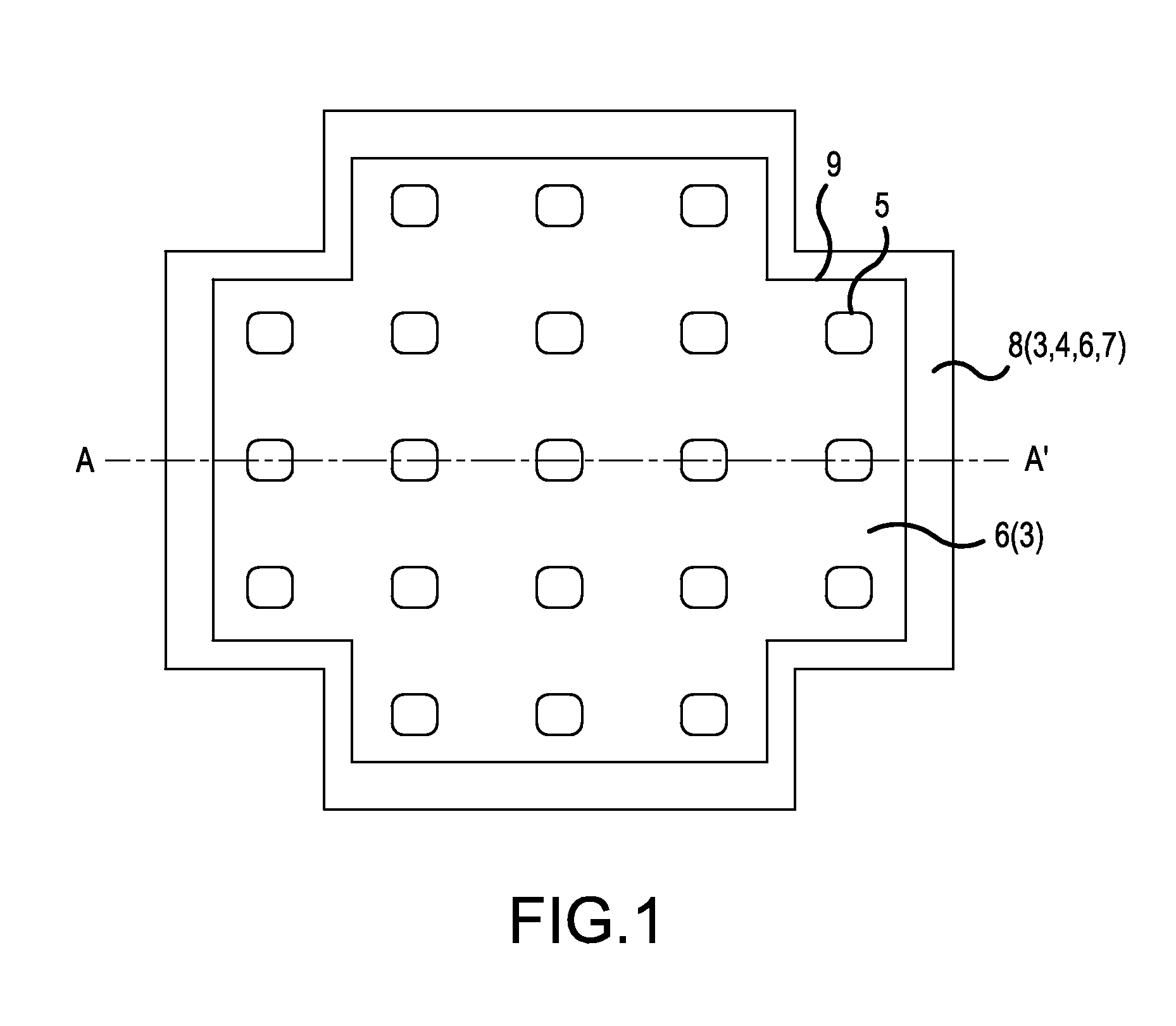
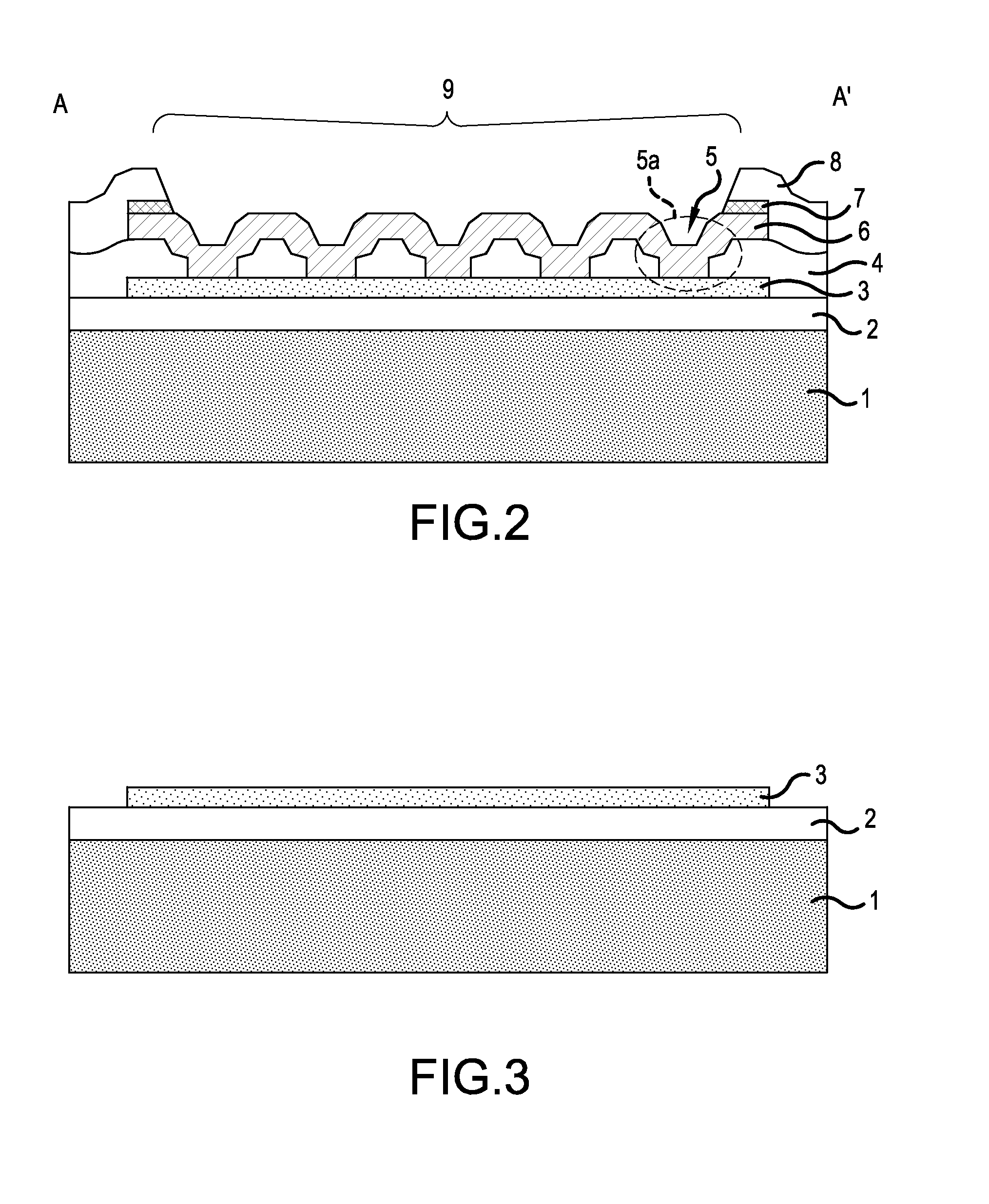
[0036]First, the planar structure of an alignment marker of a semiconductor device according to Embodiment 1 will be described. FIG. 1 is a plan view that illustrates the structure of the alignment marker of the semiconductor device according to Embodiment 1. As illustrated in FIG. 1, the alignment marker of the semiconductor device according to Embodiment 1 is configured by recessed portions 5 that are disposed on the entire face of a metal film (first metal film) 6, for example, in a matrix pattern. On the lower side (substrate side) of the metal film 6, a polysilicon film (wiring layer) 3 having a shape similar to the metal film 6, for example, a planar shape of a cross shape is disposed. The recessed portion 5 is a cavity that is formed by depressing the metal film 6 inside an opening portion formed in the interlayer insulating film 4 disposed between the metal film 6 and the polysilicon film 3.

[0037]The size of one recessed portion 5 is smaller than one pixel size of an image r...

embodiment 2

[0054]Next, the structure of an alignment marker of a semiconductor device according to Embodiment 2 will be described. FIG. 9 is a plan view that illustrates the structure of the alignment marker of the semiconductor device according to Embodiment 2. FIG. 10 is a cross-sectional view that illustrates a cross-sectional structure taken along cutting plane line B-B′ represented in FIG. 9. In the alignment marker of the semiconductor device according to Embodiment 2, there is a difference from the alignment marker of the semiconductor device according to Embodiment 1 in that one recessed portion 15 of the metal film 16 is exposed to a second opening portion 19 of the passivation film 18 and the TiN film 17. In other words, in one alignment marker, the second opening portions 19 corresponding to the number of the recessed portions 15 are disposed. In this case, in the method of manufacturing the alignment marker of the semiconductor device according to Embodiment 1, when the passivation...


PUM


Abstract

A semiconductor device has a plurality of first opening portions formed in an interlayer insulating film. The surface is covered with a metal film with a surface having concavities and convexities which scatter reflected light. Size of the first opening portion is of the same level as a contact hole of a component and cannot be recognized by an image recognition apparatus. The metal film can be recognized by the image recognition apparatus. By forming a TiN film serving as a reflection prevention film on an end of the metal film, portions that can easily scatter light and a portion that cannot easily reflect light are adjacent in an alignment marker. A passivation film is formed on the interlayer insulating film and the TiN film. Recessed portions disposed in the metal film are exposed to a second opening portion formed in the passivation film and the TiN film.

Description

BACKGROUND OF THE INVENTION[0001]A. Field of the Invention[0002]The present invention relates to a semiconductor device and a method of manufacturing a semiconductor device.[0003]B. Description of the Related Art[0004]Conventionally, active components and passive components configuring a circuit are disposed on a substrate of a semiconductor device. The active components are transistors and diodes, for example. The passive components are resistors and capacitors, for example. Furthermore, an alignment marker generally is disposed on the substrate of a semiconductor device, separately from such components. The alignment marker is used as a position recognition pattern that is used for automatically performing positioning between a photomask and a wafer when components are produced in a wafer process. In addition, the alignment marker is used as a pattern for automatically recognizing the position of a chip or the coordinates on a chip in a die-bonding process or a wire-bonding proces...

Claims


Application Information

Patent Timeline
IPC IPC(8): H01L23/544H01L23/528H01L21/768
CPCH01L23/544H01L21/76895H01L23/528H01L2223/5442H01L2223/54426H01L2223/54453H01L2924/0002
Inventor NISHIKAWA, MUTSUOFUJIMOTO, YUKOMATSUNAMI, KAZUHIRO
Owner FUJI ELECTRIC CO LTD
Learn More