
Sensor array with receiver bias electrode

a receiver bias and sensor array technology, applied in the field of electronic devices, can solve the problems of inability to detect fingerprint details, limited resolution of capacitive touch sensors, and limitations of capacitive touch sensors, and achieve the effect of improving performance and measuring more accurately

Active Publication Date: 2015-01-15
QUALCOMM INC
View PDF10 Cites 51 Cited by
  • Summary
  • Abstract
  • Description
  • Claims
  • Application Information

AI Technical Summary

Benefits of technology

The patent describes a technology for accurately measuring ultrasonic waves in a sensor or display device. By positioning the piezoelectric transmitter and receiver layers below each other, the technology enables the transmission and reception of ultrasonic signals that are perpendicular to the surface of the device, resulting in improved performance compared to devices with separate transmitter and receiver layers. This technology can be used for accurate detection and acquisition of image information, making it useful in user input detection, such as touchscreen devices. Additionally, the perpendicular transmission and reception of ultrasonic signals reduces distortion caused by the user's fingers, making it easier to detect and recognize user fingerprints.

Problems solved by technology

However, the capacitive touch sensors and fingerprint sensors have certain limitations.
For example, the resolution of capacitive touch sensors may be limited and the touch sensors may be unable to detect detailed features of a fingerprint, particularly through a cover glass of a display.
However, such capacitive devices may be incompatible with certain mobile device configurations (e.g., a relatively thick glass display or a display that occupies a large portion of the mobile device area, leaving little room for a dedicated fingerprint sensor).
In a SAW touch-sensing device, a finger of a user may distort ultrasonic signals, such as by causing phase delay and / or damping of the ultrasonic signals.

Method used


Image

  • Sensor array with receiver bias electrode
  • Sensor array with receiver bias electrode
  • Sensor array with receiver bias electrode

Examples


Embodiment Construction

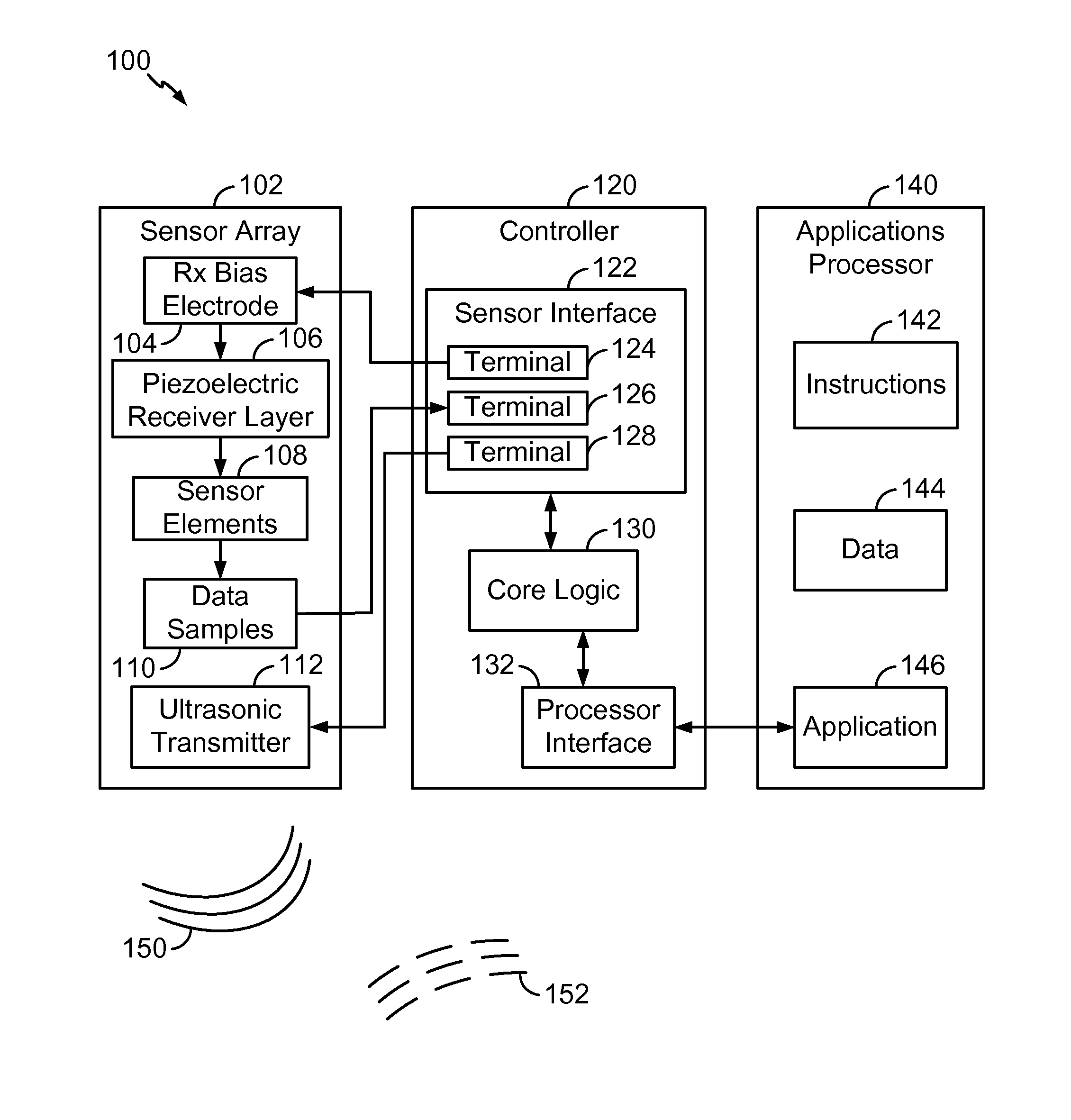
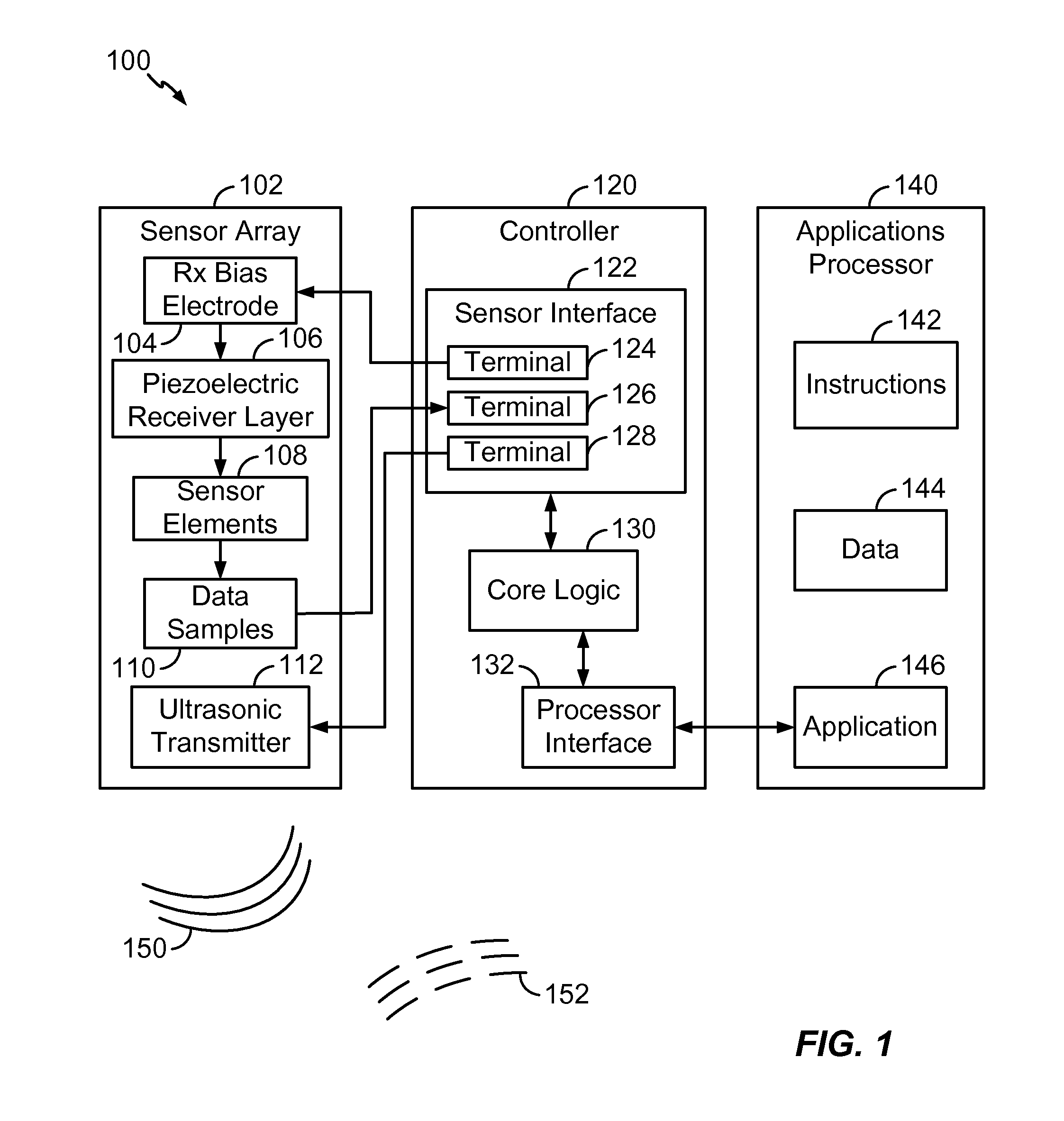
[0031]Referring to FIG. 1, a system 100 may include an ultrasonic sensor array 102, a controller 120, and an applications processor 140. The controller 120 may correspond to an integrated circuit (IC) such as an application-specific integrated circuit (ASIC), to components on one or more printed circuit boards, substrates or flexible printed circuits, or to part of another controller such as the applications processor 140. In a particular embodiment, the system 100 is integrated within an enclosure of a mobile device. For example, the sensor array 102 and the controller 120 may be integrated within or coupled to a visual display of the mobile device. In another example, the sensor array 102 and controller 120 may form part of an ultrasonic fingerprint sensor array, biometric sensor, button or touchpad, which may be included within an enclosure of the mobile device such as on an enclosure backside, sidewall, or front side near a display of the mobile device.

[0032]The sensor array 102...


PUM


Abstract

A method of operation of an ultrasonic sensor array includes receiving a receiver bias voltage at a receiver bias electrode of the ultrasonic sensor array to bias piezoelectric sensor elements of the ultrasonic sensor array. The method further includes receiving a transmitter control signal at the ultrasonic sensor array to cause an ultrasonic transmitter of the ultrasonic sensor array to generate an ultrasonic wave. The method further includes generating data samples based on a reflection of the ultrasonic wave. The receiver bias voltage and the transmitter control signal are received from an integrated circuit that is coupled to the ultrasonic sensor array.

Description

I. CROSS-REFERENCE TO RELATED APPLICATIONS[0001]The present disclosure claims priority from U.S. Provisional Patent Application No. 61 / 846,585 (Atty. Docket. No. 133605P1), U.S. Provisional Patent Application No. 61 / 846,592 (Atty. Docket. No. 133605P2), and U.S. Provisional Patent Application No. 61 / 846,604 (Atty. Docket. No. 133605P3), each filed Jul. 15, 2013 and incorporated herein by reference in its entirety.II. FIELD[0002]The present disclosure is generally related to electronic devices and more particularly to electronic devices that utilize sensing techniques, such as ultrasonic sensing techniques for biometric sensor arrays.III. DESCRIPTION OF RELATED ART[0003]Advances in technology have resulted in smaller and more powerful electronic devices and communication systems. For example, there currently exist a variety of mobile devices, such as wireless telephones, personal digital assistants (PDAs), tablet computers, and paging devices. The mobile devices may be small, lightwe...

Claims


Application Information

Patent Timeline
IPC IPC(8): G01S15/02
CPCG01S15/02G06F3/0416G06F3/043G06F3/0436G01H1/04
Inventor DICKINSON, TIMOTHYMATHE, LENNART KARL-AXELMCCARTHY, SCOTTDJORDJEV, KOSTADIN DIMITROVOLIVEIRA, LOUIS DOMINICZHOU, QUBO
Owner QUALCOMM INC
Learn More