Sequential circuit and semiconductor device

a semiconductor and circuit technology, applied in semiconductor devices, instruments, optics, etc., can solve problems such as image quality degradation, and achieve the effects of reducing transistor size, reducing on-state current, and increasing drain curren

Active Publication Date: 2014-12-11
SEMICON ENERGY LAB CO LTD
View PDF7 Cites 26 Cited by
  • Summary
  • Abstract
  • Description
  • Claims
  • Application Information

AI Technical Summary

Benefits of technology

The present invention aims to provide a semiconductor device that can reduce power consumption without reducing image quality. This is achieved by designing a capacitor that includes a metal oxide film, a pixel electrode, and a nitride insulating film. The capacitor is positioned in a pixel of the semiconductor device, and the metal oxide film and pixel electrode transmit visible light. The capacitor can have a high capacitance and allows the pixel to have a higher aperture ratio, thus reducing light loss and power consumption. Furthermore, a gate electrode on the back channel region side can prevent a negative charge and suppress a shift in the threshold voltage of a transistor in a negative direction, resulting in an increased channel formation region and a reduction in the area of the driver circuit. Overall, the present invention provides a semiconductor device that has high reliability and a reduced frame width, achieved through efficient use of light emitted from a backlight and a reduced size of semiconductor elements.

Problems solved by technology

A capacitor with small capacitance has disadvantages such as difficulty in controlling the alignment of liquid crystal molecules without decreasing driving frequency and a short period for holding a potential of an image signal, resulting in degradation in image quality.

Method used


Image

  • Sequential circuit and semiconductor device
  • Sequential circuit and semiconductor device
  • Sequential circuit and semiconductor device

Examples


example

[0349]In this example, examination results of the Vg−Id characteristics and the reliabilities of formed transistors are described.

[Formation of Samples]

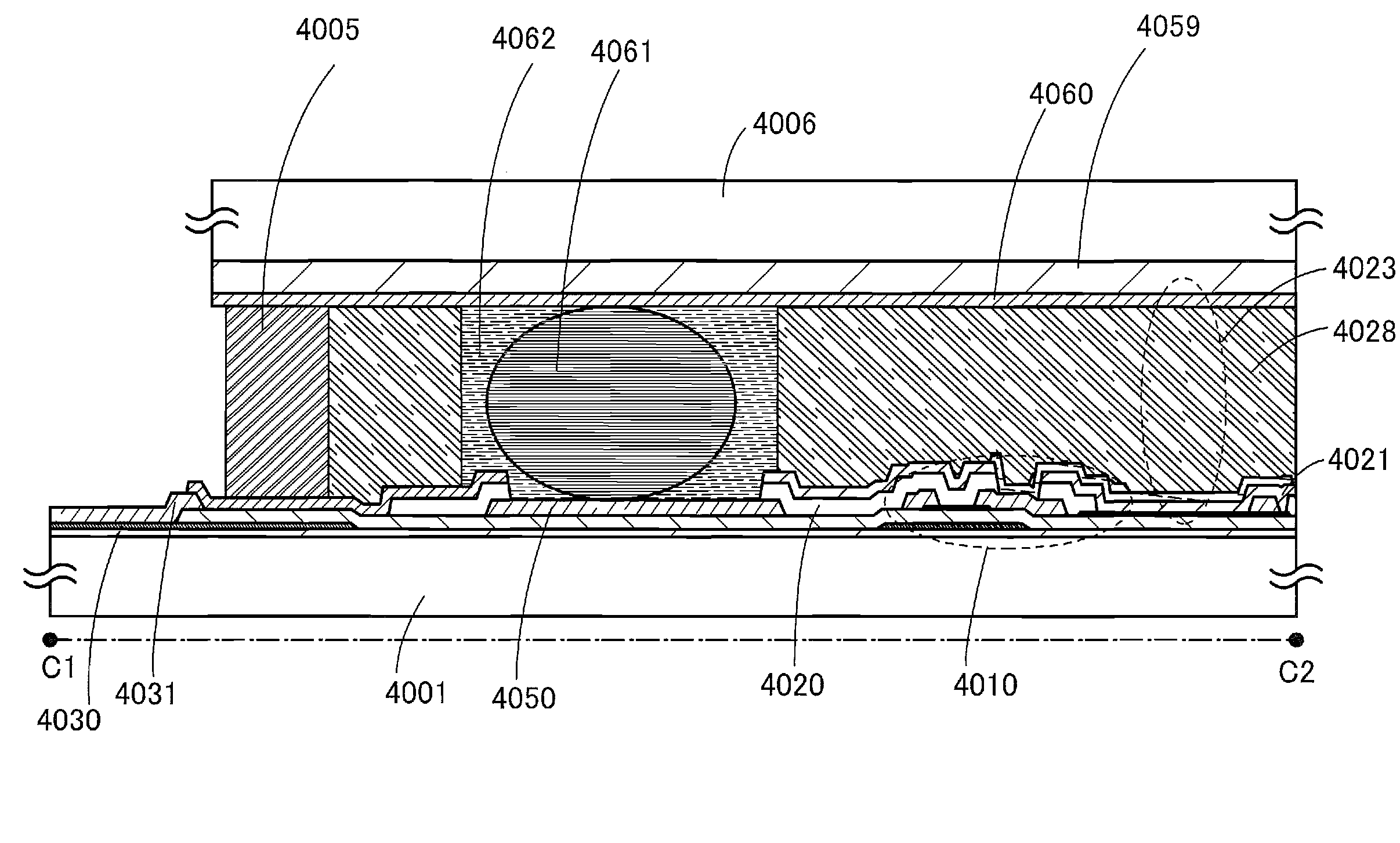
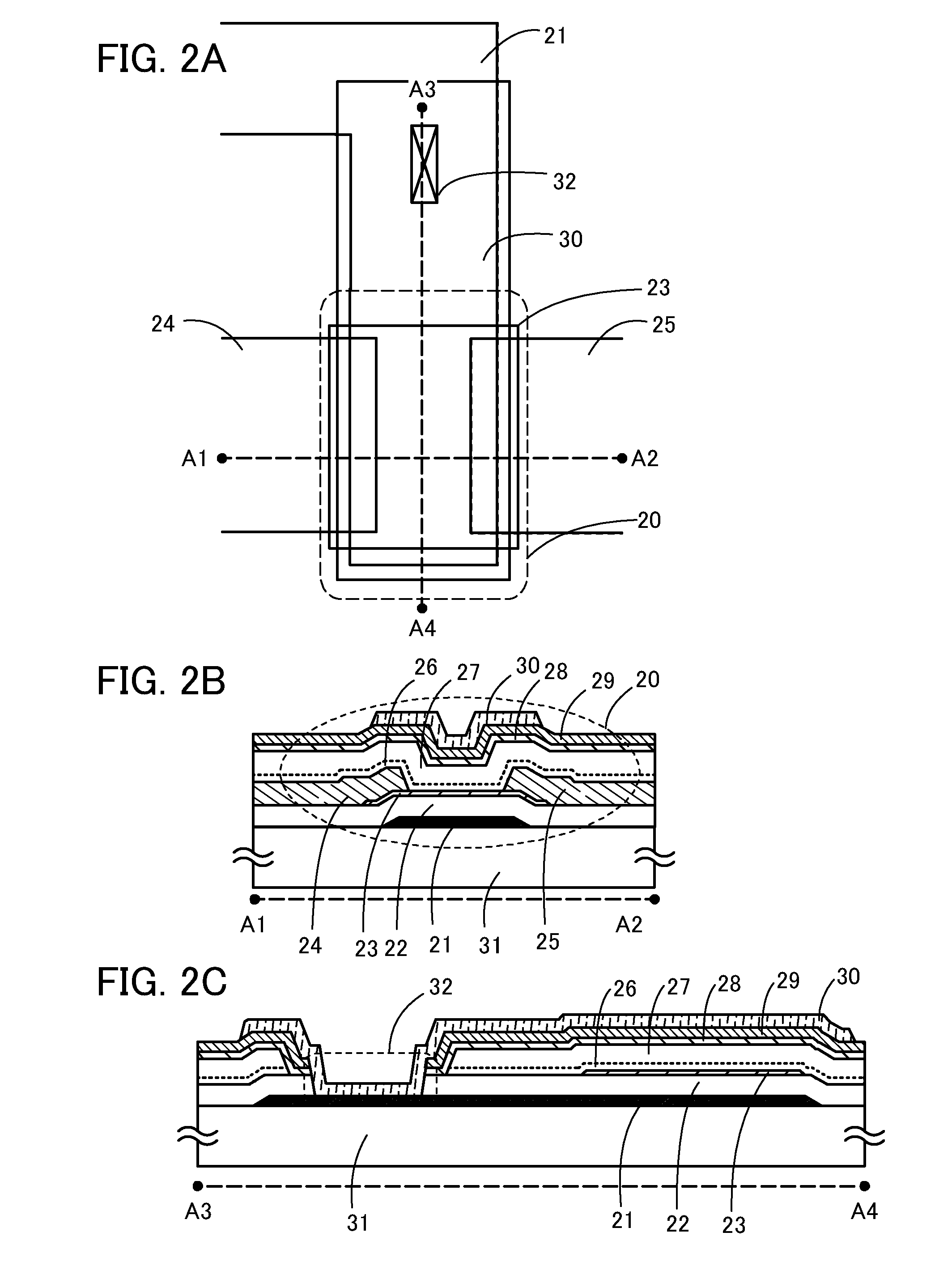
[0350]In this example, samples 1 and 2 each of which is one embodiment of the present invention, and a sample 3 for comparison were formed. Specifically, a transistor having a structure corresponding to that illustrated in FIGS. 2A to 2C was formed as the sample 1, which is one embodiment of the present invention. A transistor having a structure corresponding to that illustrated in FIGS. 19A to 19C was formed as the sample 2, which is one embodiment of the present invention. As the sample 3 for comparison, a transistor which has a structure similar to the structure illustrated in FIGS. 2A to 2C, except that the conductive film 30 was not included was formed.

[Sample 1]

[0351]First, a glass substrate was used as a substrate, and a gate electrode was formed over the substrate.

[0352]The gate electrode was formed in the following manner: a...


PUM


Abstract

The following semiconductor device provides high reliability and a narrower frame width. The semiconductor device includes a driver circuit and a pixel portion. The driver circuit has a first transistor including a first gate and a second gate electrically connected to each other with a semiconductor film sandwiched therebetween, and a second transistor electrically connected to the first transistor. The pixel portion includes a third transistor, a liquid crystal element, and a capacitor. The liquid crystal element includes a first transparent conductive film electrically connected to the third transistor, a second conductive film, and a liquid crystal layer. The capacitor includes the first conductive film, a third transparent conductive film, and a nitride insulating film. The nitride insulating film is positioned between the first transparent conductive film and the third transparent conductive film, and positioned between the semiconductor film and the second gate of the first transistor.

Description

TECHNICAL FIELD[0001]The present invention relates to a semiconductor device. In particular, the present invention relates to a sequential circuit using unipolar transistors, and a semiconductor device such as a semiconductor display device using the sequential circuit.BACKGROUND ART[0002]Semiconductor display devices, such as liquid crystal display devices and EL display devices, used in portable electronic devices have been required to reduce an area other than a pixel portion (i.e., to narrow a frame width). A system-on-panel obtained by forming a pixel portion and some of or all driver circuits over one substrate is effective in meeting the above need. In the case of the system-on-panel, like the pixel portion, the driver circuit preferably includes unipolar transistors because the panel can be manufactured at low cost. Patent Documents 1 and 2 disclose techniques for formation of various circuits such as inverters and shift registers that are used in driver circuits of semicond...

Claims


Application Information

Patent Timeline
IPC IPC(8): G02F1/1343
CPCG02F1/1343G02F1/136213G02F1/13624G02F1/13685G02F1/133345G02F1/134309G02F1/1368H01L27/1225H01L27/127H01L29/78648H01L29/7869H01L29/78696
Inventor YAMAZAKI, SHUNPEIMIYAKE, HIROYUKITOYOTAKA, KOUHEIHAYAKAWA, MASAHIKOMATSUBAYASHI, DAISUKEMATSUDA, SHINPEI
Owner SEMICON ENERGY LAB CO LTD
Why Eureka
Try Eureka