Thin film transistor and display device using the same

a thin film transistor and display device technology, applied in semiconductor devices, instruments, electrical apparatus, etc., can solve the problems of insufficient writing to pixels, easy hydrogen deficiency, and difficult to reduce the tft size for high refinement, so as to reduce parasitic capacitance, reduce parasitic capacitance, and reduce the effect of parasitic capacitan

Active Publication Date: 2014-10-16
JAPAN DISPLAY INC
View PDF3 Cites 23 Cited by
  • Summary
  • Abstract
  • Description
  • Claims
  • Application Information

AI Technical Summary

Benefits of technology

This patent is about a new type of thin film transistor that can suppress a specific issue and reduce unwanted electrical effects. This transistor can be used in a display device to produce high-quality and reliable images. The technical effect is that this transistor can improve the overall performance of the display device and ensure that it performs well even when certain protective films are applied.

Problems solved by technology

If the TFT size is reduced, insufficient writing to pixels occurs.
It is difficult to reduce the TFT size for high refinement.
(i) The IGZO film is weak against hydrogen, and hydrogen deficiency easily occurs.
However, in this structure, parasitic capacitances (Cgd, Cgd) increase between the gate electrode and the source / drain electrode.
This easily results in some problems.
However, in fact, this is very difficult in view of light diffusion or the manufacturing margin.
However, it is ascertained that, in this oxide TFT, the initial Vth is easily depleted.
Based on the inventors' examination results, in the TFT having the channel protection layer, oxygen deficiency easily occurs on the back channel side of the IGZO film, due to the damage at the film formation of the channel protection layer using plasma CVD.
As a result of the Vth depletion, the operation of the peripheral circuit is difficult, if there is any peripheral circuit incorporated in the panel.
In addition, when the voltage is negative, the energy band in the backchannel is not likely to be decreased, and the electrons are not easily induced.

Method used


Image

  • Thin film transistor and display device using the same
  • Thin film transistor and display device using the same
  • Thin film transistor and display device using the same

Examples


embodiment 1

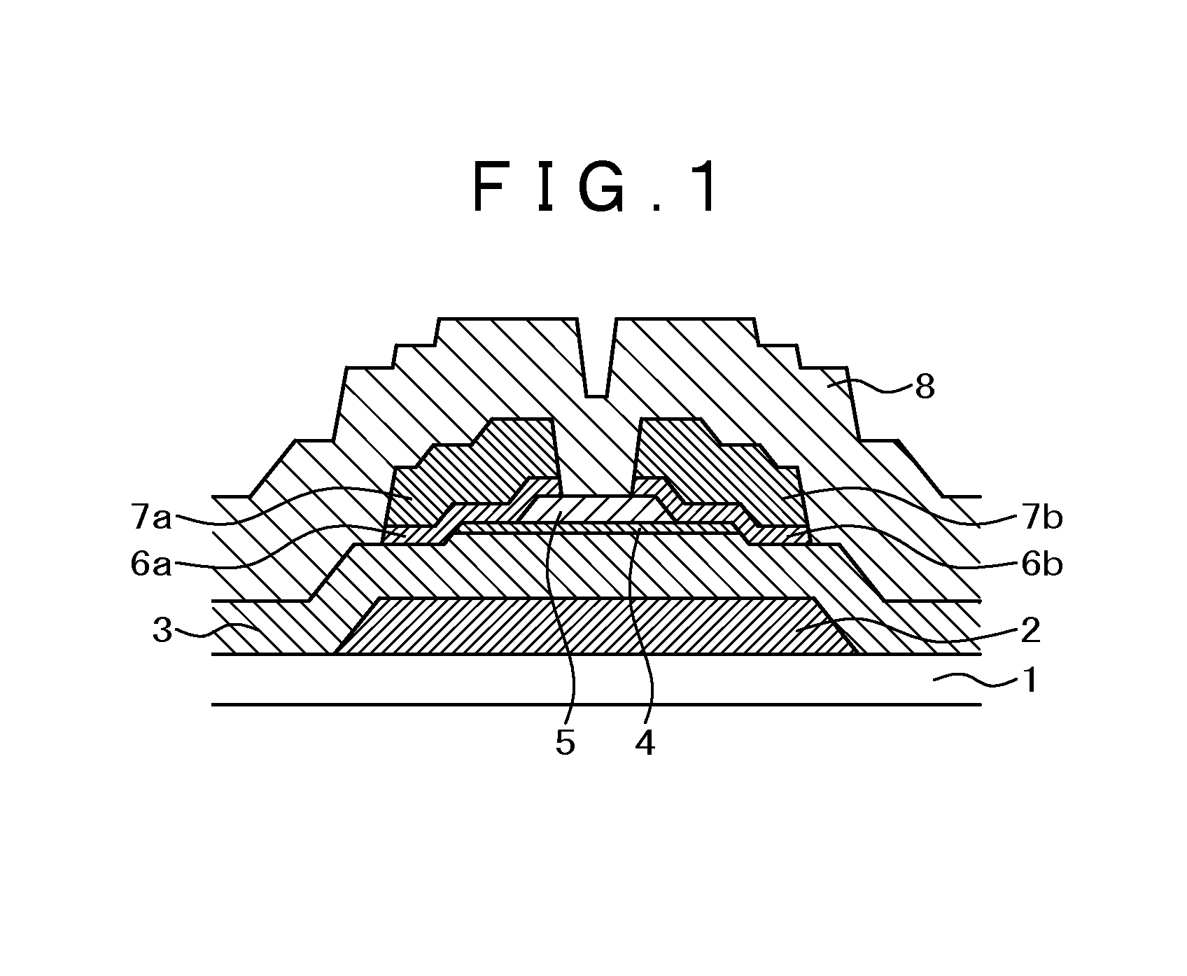
[0040]A first embodiment of the present invention will now specifically be described using FIG. 1 to FIG. 3. The same constituent elements are denoted by the same reference numerals.

[0041]First, descriptions will be made to a cross sectional structure of a thin film transistor (TFT) according to a first embodiment of the present invention. FIG. 1 is a cross sectional view of the TFT according to this embodiment. This TFT is a bottom gate TFT having a channel protection layer 5, and has a substrate 1, a gate electrode 2, a gate insulating film 3, a first oxide semiconductor layer 4 to serve as a channel layer, a channel protection layer 5, second oxide semiconductor layers 6a and 6b, a source electrode 7a, a drain electrode 7b, and a passivation film 8. In this embodiment, “7a” denotes a source electrode, while “7b” denotes a drain electrode. However, “7a” may denote the drain electrode, while “7b” may denote a source electrode. In this specification, each electrode is formed in acco...

embodiment 2

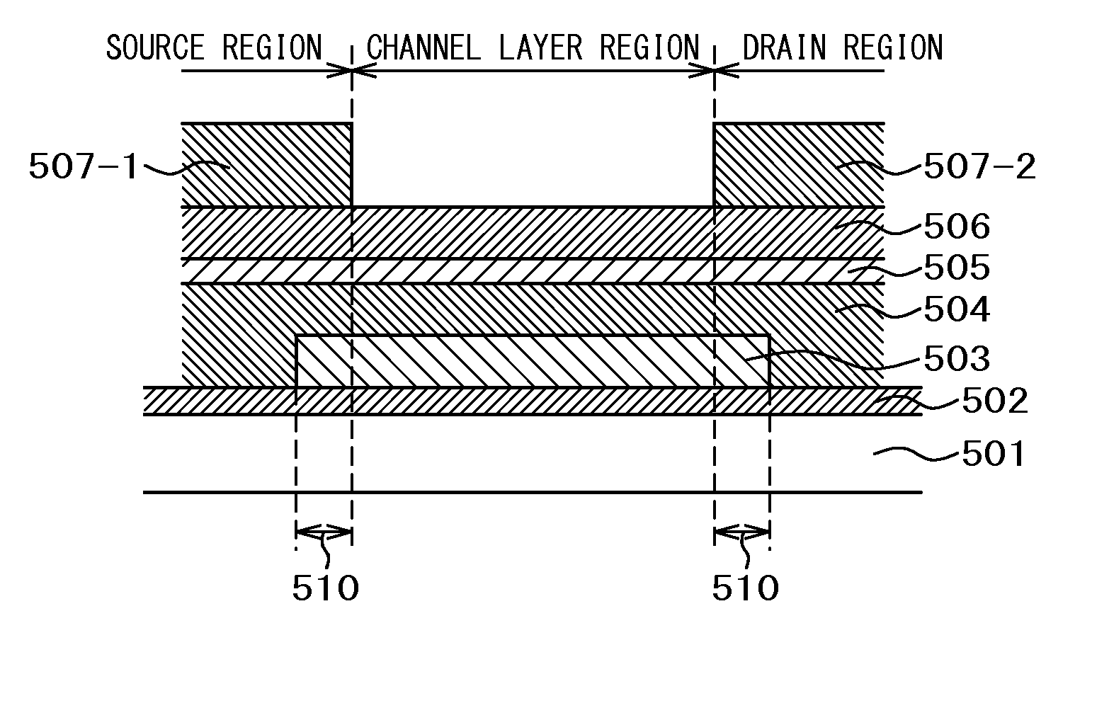
[0056]A second embodiment will now be described using FIG. 4 to FIG. 7. Those matters described in the embodiment 1 but not described in this embodiment are applicable also into this embodiment, unless there are special circumstances. FIG. 4 is a cross sectional view of a thin film transistor (TFT) according to this embodiment. In this embodiment, what differs from the embodiment 1 is that the film thickness of the first oxide semiconductor layer 4 in the source / drain region is thinner than the film thickness in the channel region. Other structural elements are the same as those of the embodiment 1, and thus will not be described again.

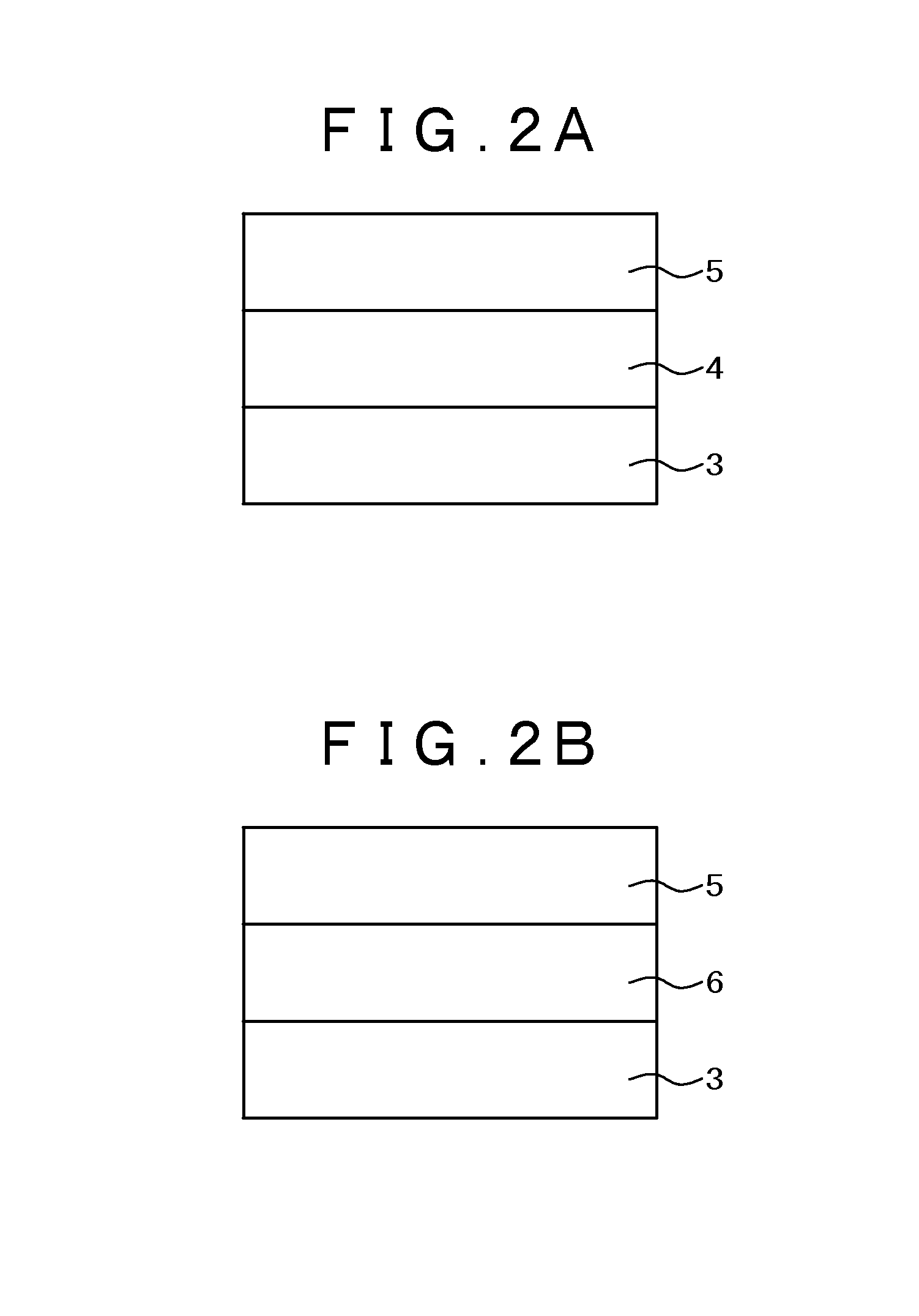
[0057]A method for manufacturing the TFT according to this embodiment will be described using FIG. 5A to FIG. 5D.

[0058]FIG. 5A to FIG. 5D illustrate procedures for manufacturing the TFT according to this embodiment (illustrate only the main parts of the TFT). This TFT is also a bottom gate TFT having a channel protection layer. The typical manufacturi...

embodiment 3

[0110]Descriptions will now be made to a third embodiment of the present invention using FIG. 8. Those matters described in the embodiment 1 or the embodiment 2 but not described in this embodiment are applicable also into this embodiment, unless there are special circumstances.

[0111]FIG. 8 is a cross sectional view of a thin film transistor (TFT) according to this embodiment. In the TFT according to this embodiment, what differs from the TFT illustrated in FIG. 1 is that a third oxide semiconductor layer 101a as a source contact layer is formed between the second oxide semiconductor layer 6a and the source electrode wiring 7a, in the source region. In addition, a third oxide semiconductor layer 101b as a drain contact layer is formed between the oxide semiconductor layer 6b and the drain electrode wiring 7b, in the drain region. Other elements are the same as the above, and thus will not be described again.

[0112]The source contact layer 101a and the drain contact layer 101b in the ...


PUM


Abstract

In a bottom gate thin film transistor using a first oxide semiconductor layer as a channel layer, the first oxide semiconductor layer and second semiconductor layers include In and O. An (O / In) ratio of the second oxide semiconductor layers is equal to or larger than that of the first oxide semiconductor layer, and a film thickness thereof is thicker than that of the first oxide semiconductor layer.

Description

CLAIM OF PRIORITY[0001]The present application claims priority from Japanese patent application JP 2013-083282 filed on Apr. 11, 2013 the content of which is hereby incorporated by reference into this application.FIELD OF THE INVENTION[0002]The present invention relates to a thin film transistor using an oxide semiconductor as a channel layer, and also a display device using the same.BACKGROUND OF THE INVENTION[0003]In display devices, there are arranged a TFT substrate and an opposite substrate. The TFT substrate has pixels which are formed in matrix and each of which has a pixel electrode and a thin film transistor (TFT). The opposite substrate is opposed to the TFT substrate, and has a color filter or the like in a position corresponding to the pixel electrode of the TFT substrate. In liquid crystal display devices, liquid crystal is sandwiched between the TFT substrate and the opposite substrate. Light transmittance by liquid crystal molecules is controlled in association with e...

Claims


Application Information

Patent Timeline
Patent Type & Authority Applications(United States)
IPC IPC(8): H01L29/786H01L27/12
CPCH01L27/1225H01L29/78693H01L29/78618G02F1/133357G02F1/133345G02F1/133512G02F1/133514G02F1/1337G02F1/134309G02F1/1368H01L27/1285H01L29/24H01L29/78606H01L29/78633H01L29/7869H01L29/78696
Inventor SUZUMURA, ISAOUEMURA, NORIHIRONODA, TAKESHIMIYAKE, HIDEKAZUYAMAGUCHI, YOHEI
Owner JAPAN DISPLAY INC
Why Eureka
Try Eureka