
Wafer scale epitaxial graphene transfer

a graphene transfer and wave-scale technology, applied in the direction of graphene, solid-state devices, layered products, etc., can solve the problems of difficult control and incorporation into semiconductor processing, difficult processing of graphene, and inability to produce uniform graphene films

Inactive Publication Date: 2014-10-02
ELPIS TECH INC
View PDF6 Cites 24 Cited by
  • Summary
  • Abstract
  • Description
  • Claims
  • Application Information

AI Technical Summary

Benefits of technology

The patent describes a method for transferring a two-dimensional material, such as graphene, from one substrate to another. The method involve forming a layer of the material on a substrate, adding a layer of stress to the top layer of the material, and then exfoliating the material from the substrate. This process can allow for the transfer of a single layer of the material onto another substrate, which can be useful for making devices with graphene or other two-dimensional materials. The patent also describes a specific method for transferring graphene onto a silicon carbide substrate. Overall, the patent provides a way to efficiently and accurately transfer high-quality two-dimensional materials onto different substrates for use in various applications.

Problems solved by technology

Processing of graphene is often unconventional relative to traditional processing techniques and is often difficult to control and incorporate into semiconductor processing.
This technique may not produce a uniform graphene film.
Exfoliation and transfer of the graphene layer is often very difficult.
However, exfoliation and transfer of the graphene layer is very difficult.
Another disadvantage of CVD growth on metal substrates is that the grown graphene layer is a poly-crystal.

Method used


Image

  • Wafer scale epitaxial graphene transfer
  • Wafer scale epitaxial graphene transfer
  • Wafer scale epitaxial graphene transfer

Examples


Embodiment Construction

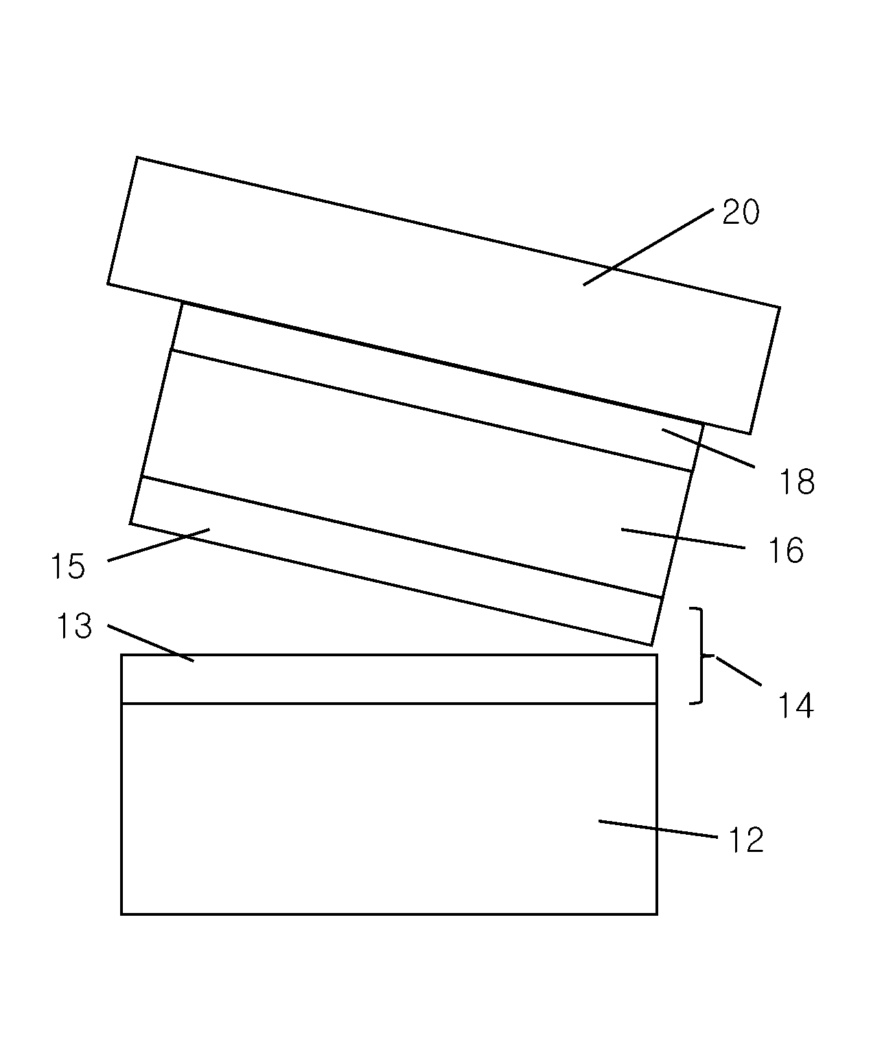
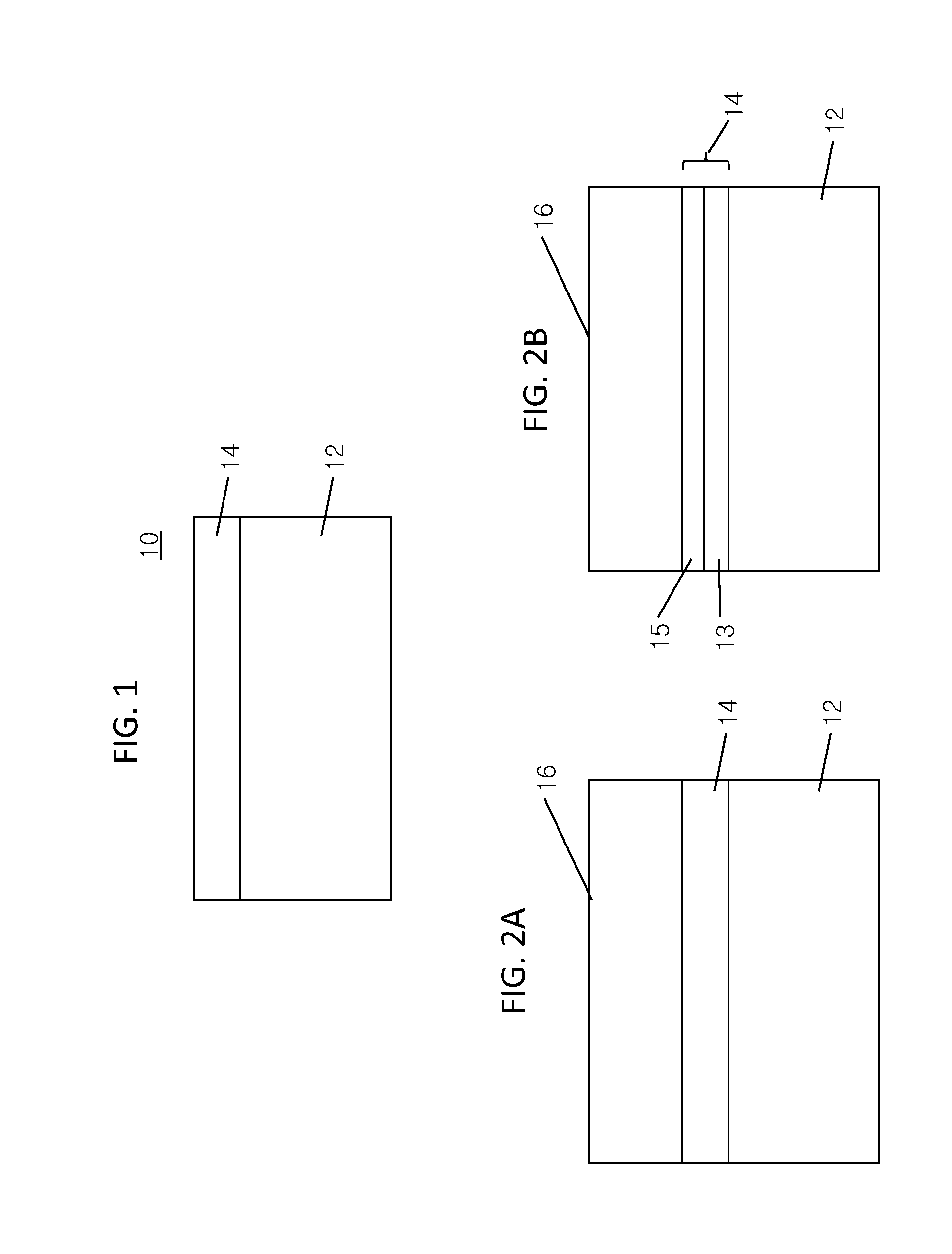
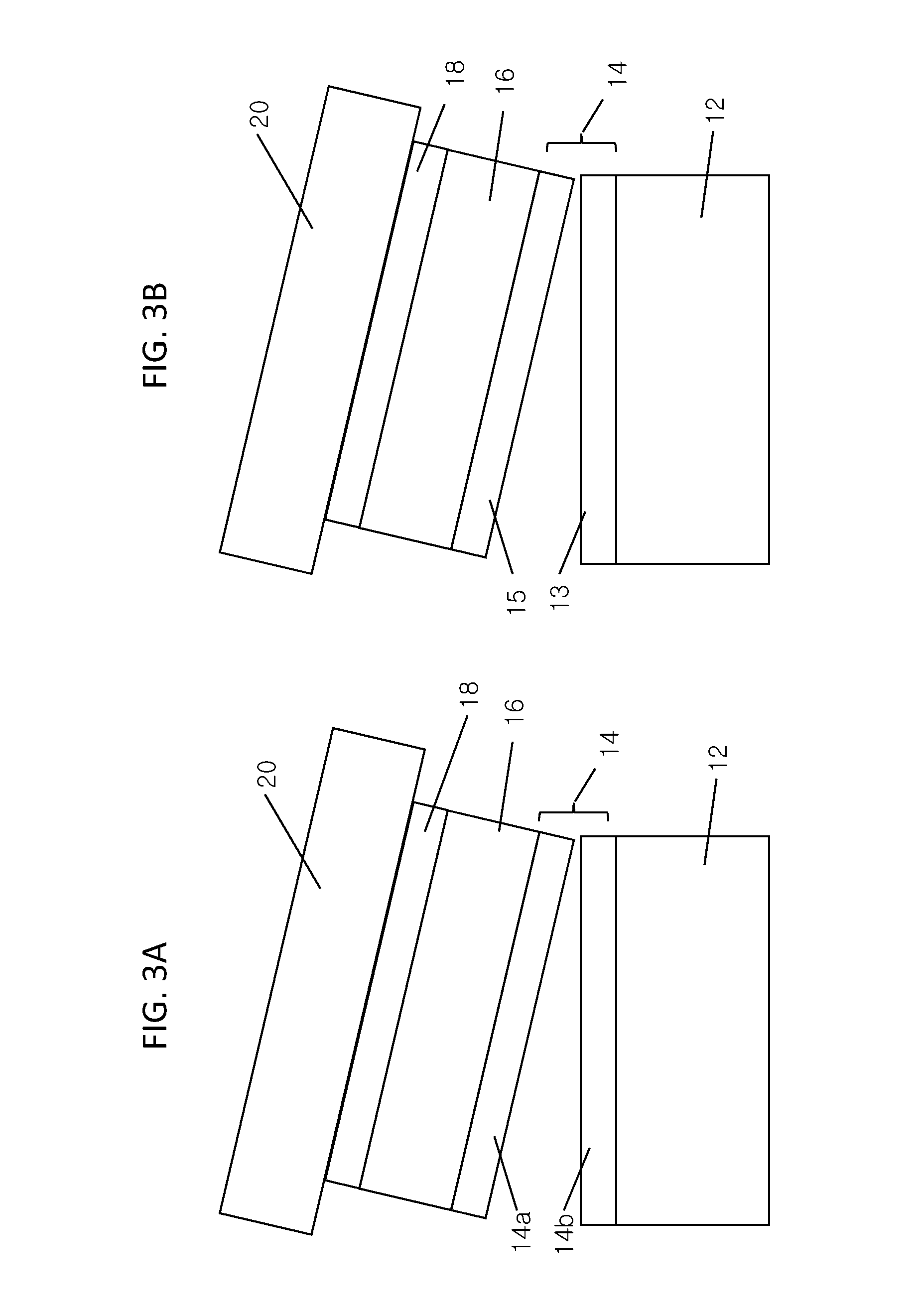
[0021]In accordance with the present principles, methods for transferring large sections of two-dimensional (2D) materials are provided. In one embodiment, a 2D material is provided on a substrate having a thickness of one or more monolayers. In one embodiment, the 2D material includes graphene and the substrate may include SiC. A stressor layer is formed on the 2D material and a handle substrate is bonded to the stressor layer. The stressor layer induces stress in at least the closest monolayer. Since the 2D material relies on weak Van der Waals forces to hold the monolayers together, the 2D material may be chemically bonded to the substrate. The stressor layer grips at least the closest monolayer, and lifting the handle substrate results in a high-quality mechanical exfoliation and lift-off of at least the closest monolayer. The top monolayer can be lifted off with little or no damage. The stressor layer may now be employed for further processing, or the exfoliated monolayer of th...


PUM

PropertyMeasurementUnit
pressuresaaaaaaaaaa
temperatureaaaaaaaaaa

Abstract

A method for transfer of a two-dimensional material includes forming a spreading layer of a two-dimensional material on a substrate, the spreading layer having a monolayer. A stressor layer is formed on the spreading layer, and the stressor layer is configured to apply stress to a closest monolayer of the spreading layer. The closest monolayer is exfoliated by mechanically splitting the spreading layer wherein the closest monolayer remains on the stressor layer.

Description

BACKGROUND[0001]1. Technical Field[0002]The present invention relates to semiconductor devices and fabrication, and more particularly to methods and devices for separating monolayers in a layer of graphene using a stressor layer.[0003]2. Description of the Related Art[0004]Microelectronics applications have been increasingly employing graphene devices due to their conductive, mechanical and other properties. Processing of graphene is often unconventional relative to traditional processing techniques and is often difficult to control and incorporate into semiconductor processing. Graphene may be obtained using many techniques. One popular technique includes micro-mechanical alleviation of graphite. This includes employing adhesive tape to repeatedly split graphite crystals into increasingly thinner pieces. The tape with attached optically transparent flakes is dissolved in acetone, and the flakes including monolayers were sedimented on a silicon wafer. This has been improved by dry d...

Claims


Application Information

Patent Timeline
Patent Type & Authority Applications(United States)
IPC IPC(8): H01L21/02B32B43/00
CPCB32B43/006H01L21/02376H01L29/1606H01L21/2007C01B32/184H01L21/02002Y10T156/11Y10T156/1153H01L21/6835H01L2221/68381H01L2221/68368H01L21/0272H01L21/02527H01L21/02378H01L2221/68345
Inventor BEDELL, STEPHEN W.DIMITRAKOPOULOS, CHRISTOS D.FOGEL, KEITH E.HANNON, JAMES B.KIM, JEEHWANPARK, HONGSIKPFEIFFER, DIRKSADANA, DEVENDRA K.
Owner ELPIS TECH INC
Learn More