SiC SUBSTRATE WITH SiC EPITAXIAL FILM
a technology of silicon carbide substrate and epitaxial film, which is applied in the direction of crystal growth process, polycrystalline material growth, and test/measurement of semiconductor/solid-state devices, etc., can solve the problems of non-operational semiconductor devices, known to limit or destroy the operation of semiconductor devices formed, and unique challenges of wafer substrates. achieve good adhesion
- Summary
- Abstract
- Description
- Claims
- Application Information
AI Technical Summary
Benefits of technology
Problems solved by technology
Method used
Image
Examples
example 1
[0077]A warm wall CVD system capable of processing 5 pcs of 76 mm diameter substrates was used for epitaxial growth.
[0078]The substrates used were 4H-SiC polytype, tilted 4 degrees away from the c-axis to the direction. The substrates had resistivity in the range 0.015 to 0.030 ohm-cm.
[0079]A new set of graphite consumables was loaded, baked and coated with a SiC layer as described. The substrates were loaded and processed. The process details and the results measured on a wafer from the process are:[0080]Run ID / Wafer ID: 1241_AV1006-09[0081]Growth temperature: 1585° C.[0082]Pressure: 124 mbar[0083]Total Hydrogen flow: 72.4 slpm[0084]Film Thickness: 5.53 μm, within wafer range 8.1%[0085]Growth temperature: 1585° C.[0086]Pressure: 124 mbar[0087]Total H2 flow: 72.4 slpm[0088]Doping: 5.5×10¹⁵ / cm3, within wafer range 15%.[0089]Defect density: 0.4 cm−2 [0090]RMS roughness 0.61 nm
example 2
[0091]A warm wall CVD system capable of processing 10 pcs of 100 mm diameter substrates was used for epitaxial growth.
[0092]The substrates used were 4H-SiC polytype, tilted 4 degrees to the direction. The substrates had resistivity in the range 0.015 to 0.030 ohm-cm.
[0093]A new set of graphite consumables was loaded, baked and coated with a SiC layer as described. The substrates were loaded and processed. The process details and the results measured on a wafer from the process are:[0094]Run ID / Wafer ID: A0971_AN2152-16[0095]Growth temperature: 1530° C.[0096]Pressure: 200 mbar[0097]Total H2 flow: 126 slpm[0098]Film Thickness: 7 μm, within wafer range 6.4%[0099]Film Doping: 5.7×10¹⁵ / cm3, within wafer range 15.7%[0100]Defect density: 0.83 cm−2 [0101]RMS roughness 0.30 nm
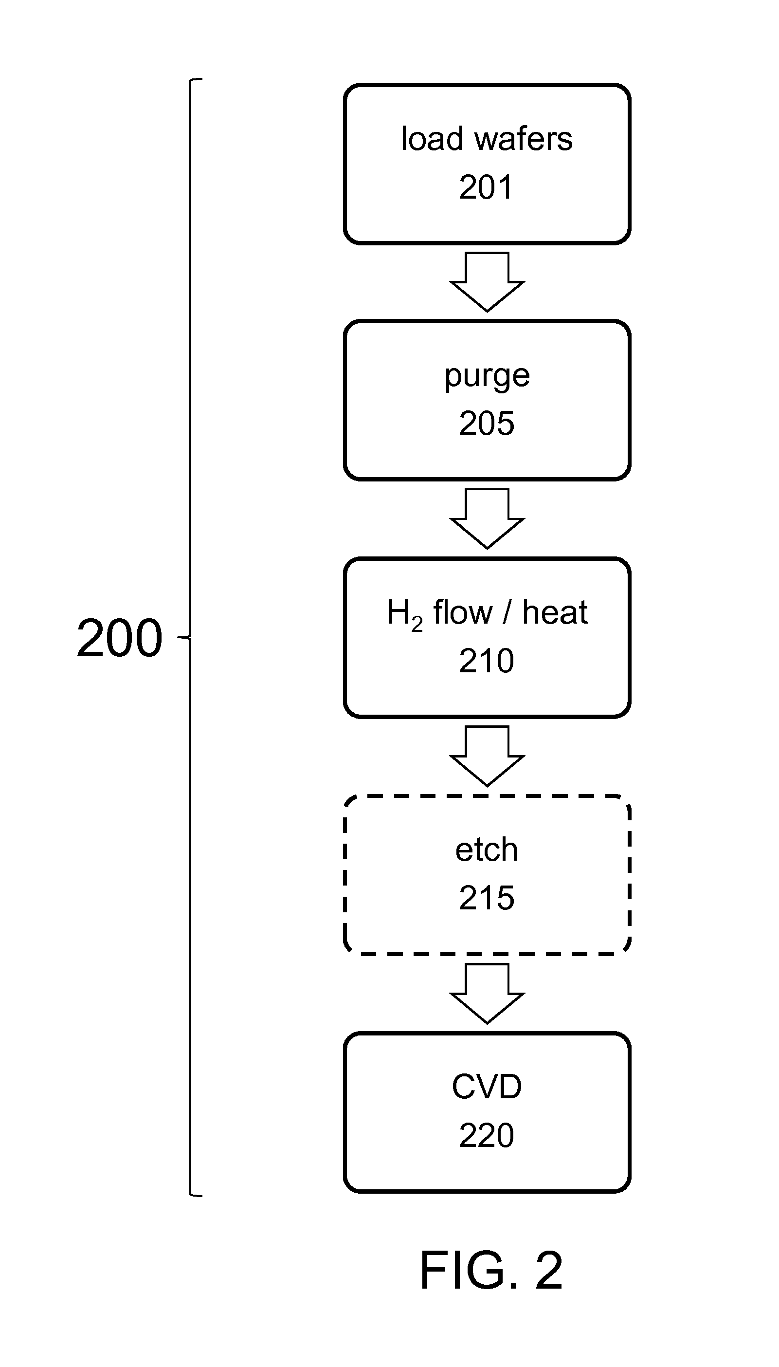
[0102]FIGS. 3, 4 and 5 depict an example of a method 300 of forming an epitaxial SiC film on a plurality of SiC substrates. The SiC substrates can be positioned on a susceptor in a warm wall CVD system, the warm wall CV...
PUM
| Property | Measurement | Unit |
|---|---|---|
| temperature | aaaaa | aaaaa |
| pressure | aaaaa | aaaaa |
| temperature | aaaaa | aaaaa |
Abstract
Description
Claims
Application Information
 - R&D
- Intellectual Property
- Life Sciences
- Materials
- Tech Scout
- Unparalleled Data Quality
- Higher Quality Content
- 60% Fewer Hallucinations
Browse by: Latest US Patents, China's latest patents, Technical Efficacy Thesaurus, Application Domain, Technology Topic, Popular Technical Reports.
© 2025 PatSnap. All rights reserved.Legal|Privacy policy|Modern Slavery Act Transparency Statement|Sitemap|About US| Contact US: help@patsnap.com


