
Wafer carrier with temperature distribution control

Inactive Publication Date: 2014-09-18
VEECO INSTR
View PDF4 Cites 34 Cited by
  • Summary
  • Abstract
  • Description
  • Claims
  • Application Information

AI Technical Summary

Benefits of technology

The invention provides a way to deliver a uniform gas to multiple wafers in a carrier to promote efficient heat transfer and uniformity of temperatures. The gas delivered has a high conductivity, enhancing heat transfer and reducing sensitivity to variations in thermal conductivity. The gas is delivered through weep orifices distributed in a matrix pattern to ensure uniform distribution. The plenum configurations and distribution manifold arrangements prevent starvation of the weep orifices. These technical effects improve heat transfer performance and achieve more consistent temperatures across a wafer or between multiple wafers.

Problems solved by technology

It has been found that such an arrangement can cause localized heating or cooling of the wafer at locations immediately above the exit aperture.
Localized heating or cooling adversely affects the temperature profile of exposed face of the wafer, and can also cause the wafer to bow slightly due to the presence of thermal gradients.

Method used


Image

  • Wafer carrier with temperature distribution control
  • Wafer carrier with temperature distribution control
  • Wafer carrier with temperature distribution control

Examples


Embodiment Construction

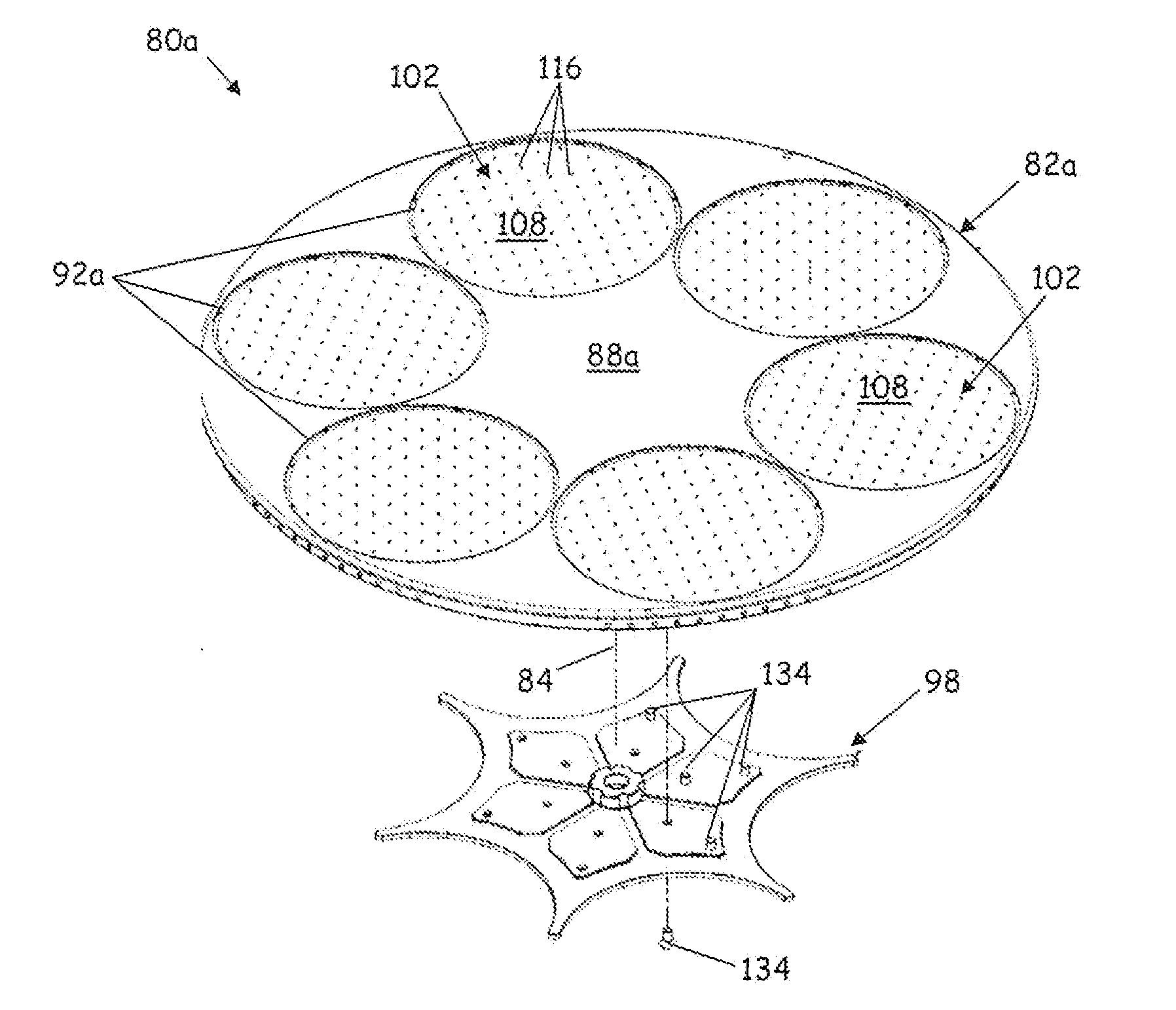
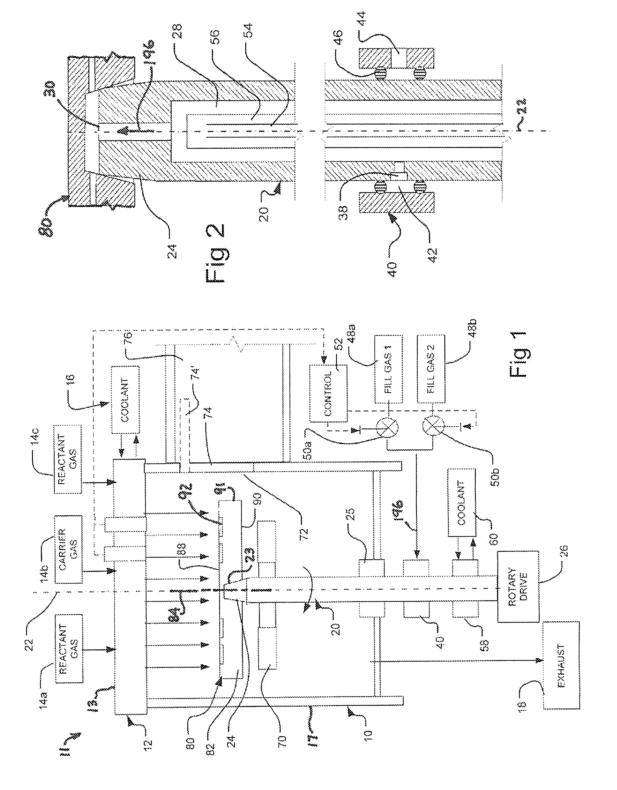
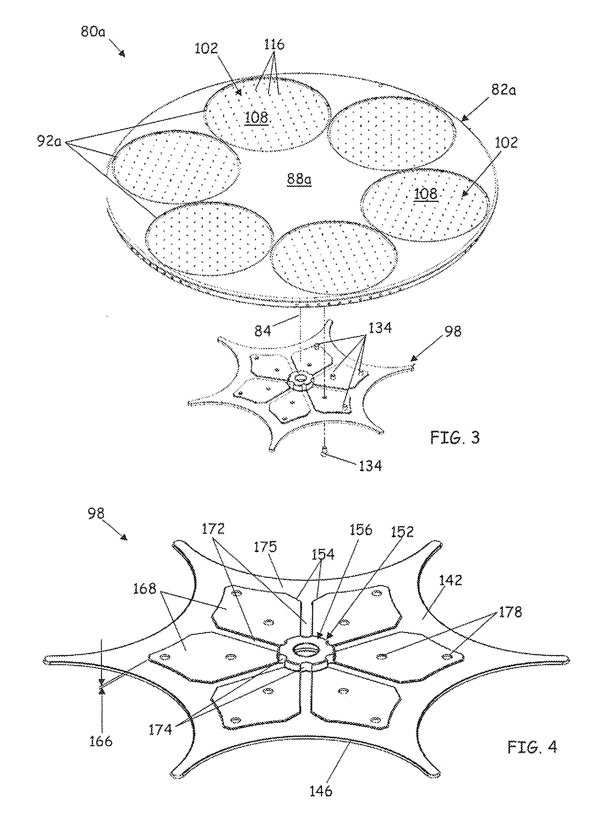
[0038]Referring to FIGS. 1 and 2, a schematic of a chemical vapor deposition (CVD) apparatus 11 is depicted an embodiment of the invention. The CVD apparatus 11 includes a reaction chamber 10 having a gas distribution element 12 arranged at a top end 13 of the reaction chamber 10. In certain embodiments, the gas distribution element 12 is connected to sources 14a, 14b, 14c for supplying process gases to be used in the wafer treatment process, such as a carrier gas and reactant gases such as a metalorganic compound and a source of a group V metal. The gas distribution element 12 is arranged to receive the various gases and direct a flow of process gasses generally in the downward direction. The gas distribution element 12 can also be connected to a coolant system 16 arranged to circulate a liquid through the gas distribution element 12 so as to maintain the temperature of the element at a desired temperature during operation. A similar coolant arrangement (not depicted) can be provid...


PUM

PropertyMeasurementUnit
Temperatureaaaaaaaaaa
Flow rateaaaaaaaaaa
Diameteraaaaaaaaaa

Abstract

Wafer carrier arranged to hold a plurality wafers and to inject a fill gas into gaps between the wafers and the wafer carrier for enhanced heat transfer and to promote uniform temperature of the wafers. The apparatus is arranged to vary the composition, flow rate, or both of the fill gas so as to counteract undesired patterns of temperature non-uniformity of the wafers. In various embodiments, the wafer carrier utilizes at least one plenum structure contained within the wafer carrier to source a plurality of weep holes for passing a fill gas into the wafer retention pockets of the wafer carrier. The plenum(s) promote the uniformity of the flow, thus providing efficient heat transfer and enhanced uniformity of wafer temperatures.

Description

FIELD OF THE INVENTION[0001]The invention relates generally to semiconductor fabrication technology and, more particularly, to chemical vapor deposition (CVD) processing and associated apparatus for reducing temperature non-uniformities on semiconductor wafer surfaces.BACKGROUND OF THE INVENTION[0002]Many semiconductor devices are formed by processes performed on a substrate. For example, in the fabrication of light-emitting diodes (LEDs) and other high-performance devices such as laser diodes, optical detectors, and field effect transistors, a chemical vapor deposition (CVD) process is typically used to grow a thin film stack structure using materials such as gallium nitride over a sapphire or silicon substrate. The substrate typically is slab of a crystalline material, commonly referred to as a “wafer,” typically in the form of a disc.[0003]One common process is epitaxial growth. For example, devices formed from compound semiconductors such as III-V semiconductors typically are fo...

Claims


Application Information

Patent Timeline
IPC IPC(8): C30B25/12C30B25/10
CPCC30B25/10C30B25/12C23C16/458C23C16/4586C30B29/40Y10T137/0318
Inventor KRISHNAN, SANDEEPGURARY, ALEXANDER I.MOY, KENG
Owner VEECO INSTR
Learn More