Method and image processing device for image dynamic range compression with local contrast enhancement
- Summary
- Abstract
- Description
- Claims
- Application Information
AI Technical Summary
Benefits of technology
Problems solved by technology
Method used
Image

Examples
first embodiment
The First Embodiment
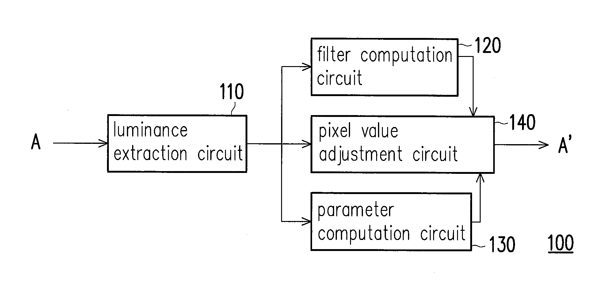
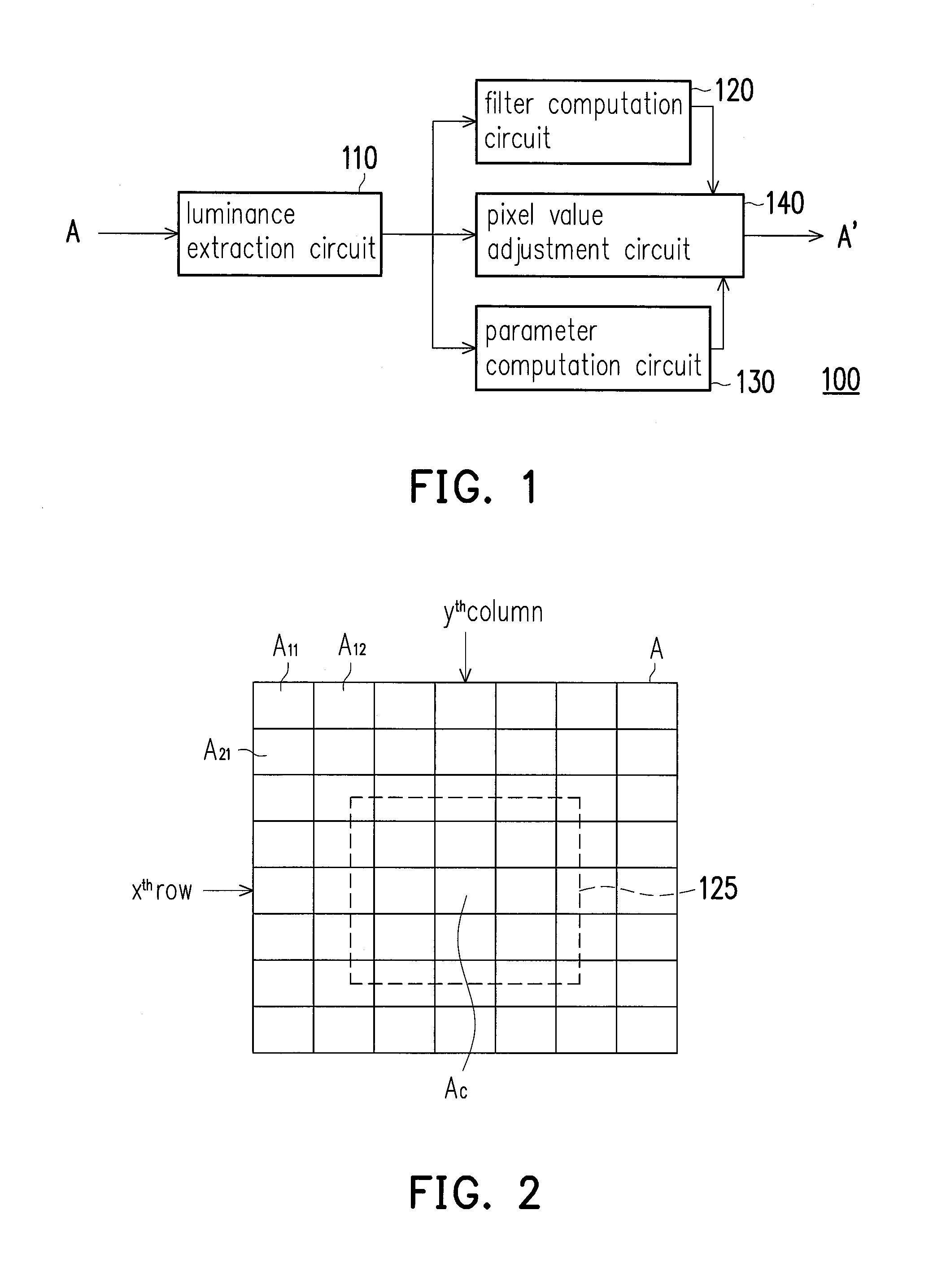
[0040]FIG. 1 depicts a block schematic diagram of an image processing device according to an exemplary embodiment of the present invention. It should, however, be noted that this is merely an illustrative example and the present invention is not limited in this regard. All components of the image processing device and their configurations are first introduced in FIG. 1. The detailed functionalities of the components are disclosed along with FIG. 2.
[0041]Referring to FIG. 1, an image processing device 100 in the present embodiment receives an image A and outputs an image A′. The image processing device 100 performs dynamic range compression with local contrast enhancement on the image A so as to enhance detail of the image A, wherein an output of the image processing device 100 is the image A′. The image processing device 100 may be a personal computer, a laptop computer, a digital camera, a digital camcorder, a web camera, a smart phone, a tabular computer, a sca...
second embodiment
The Second Embodiment
[0069]The second embodiment is similar to the first embodiment, and therefore only the differences will be described herein. In the second embodiment, the functionality of a pixel value adjustment circuit may be implemented as a three-dimensional luminance lookup table (3D LLUT) so as to accelerate the computation.
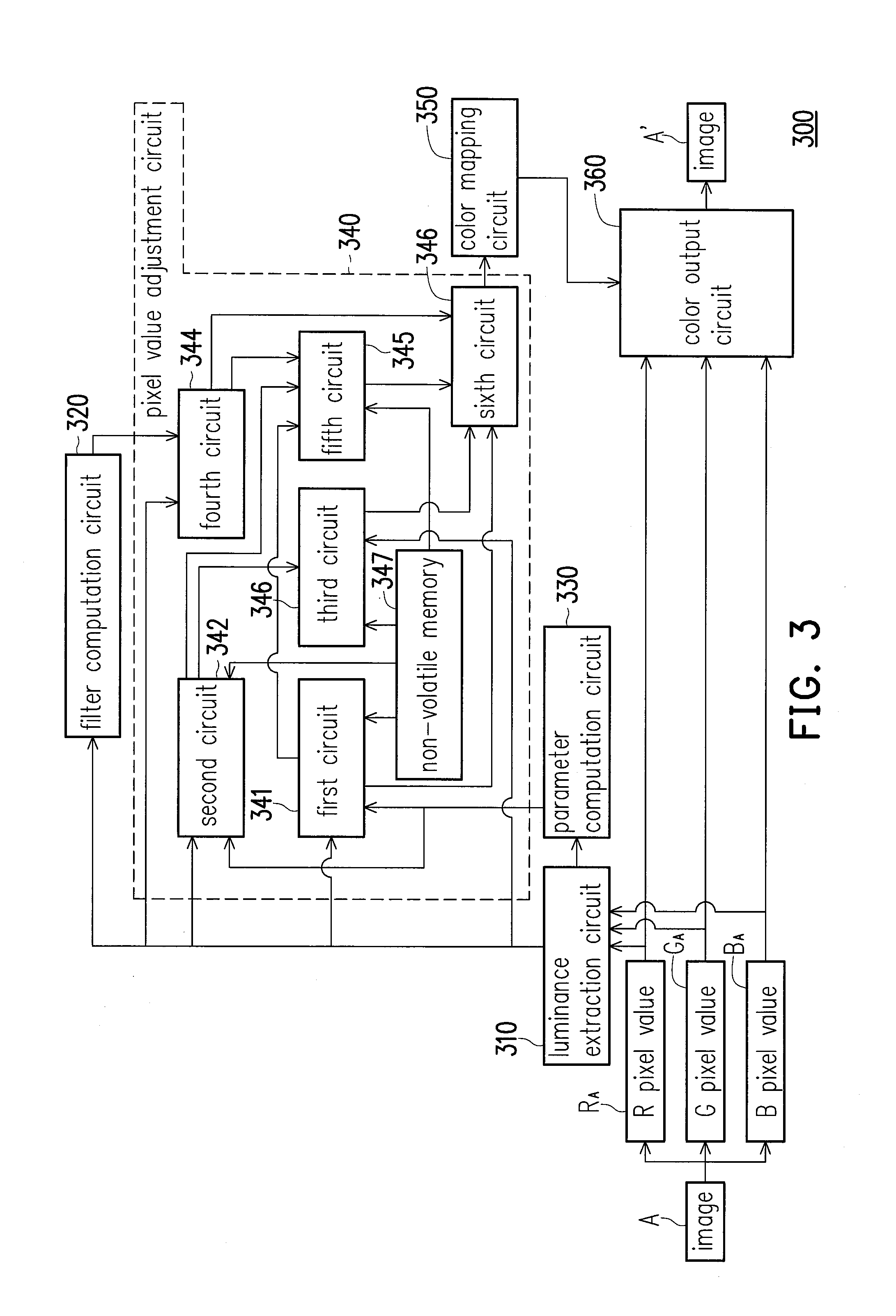
[0070]FIG. 5 depicts a block diagram of an image processing device according to the second embodiment of the present invention. Referring to FIG. 5, an image processing device 500 includes the luminance extraction circuit 310, the filter computation circuit 320, the parameter computation circuit 330, a pixel value adjustment circuit 540, the color mapping circuit 350, and the color output circuit 360, wherein the functionalities of the luminance extraction circuit 310, the filter computation circuit 320, the parameter computation circuit 330, the color mapping circuit 350, and the color output circuit 360 have been explained in detail in the first embo...
third embodiment
The Third Embodiment
[0075]The third embodiment is similar to the second embodiment, and therefore only the difference will be described herein. In the third embodiment, the functionality of a pixel value adjustment circuit may be implemented as a 2-dimensional luminance lookup table (2D LLUT) so as to reduce the memory usage.
[0076]FIG. 6 depicts a block schematic diagram of an image processing device according to the third embodiment of the present invention. Referring to FIG. 6, an image processing device 600 includes the luminance extraction circuit 310, the filter computation circuit 320, the parameter computation circuit 330, a pixel value adjustment circuit 640, the color mapping circuit 350, and the color output circuit 360, wherein the functionalities of the luminance extraction circuit 310, the filter computation circuit 320, the parameter computation circuit 330, the color mapping circuit 350, and the color output circuit 360 have been explained in detail in the first embod...
PUM
 Abstract
Description
Claims
Application Information
 - R&D
- Intellectual Property
- Life Sciences
- Materials
- Tech Scout
- Unparalleled Data Quality
- Higher Quality Content
- 60% Fewer Hallucinations
Browse by: Latest US Patents, China's latest patents, Technical Efficacy Thesaurus, Application Domain, Technology Topic, Popular Technical Reports.
© 2025 PatSnap. All rights reserved.Legal|Privacy policy|Modern Slavery Act Transparency Statement|Sitemap|About US| Contact US: help@patsnap.com