
Shallow trench isolation integration methods and devices formed thereby

a technology of integrated methods and trenches, applied in the field of semi-torque isolation integration methods/schemes, can solve the problems of poor device performance, fin damage, severe sti-oxide recesses discovered in downstream processes, etc., and achieve enhanced high aspect ratio process, high density, and high aspect ratio

Active Publication Date: 2014-08-14
GLOBALFOUNDRIES US INC
View PDF7 Cites 51 Cited by
  • Summary
  • Abstract
  • Description
  • Claims
  • Application Information

AI Technical Summary

Benefits of technology

The present invention provides methods for manufacturing semiconductor devices using multiple layers and protective liners between them. These methods involve etching set of trenches in a substrate, depositing layers over the trenches, and filling the trenches with a high aspect ratio process material, which is then polished and etched back. The invention also includes methods for removing the layers and refilling the trenches with a high density plasma material. The technical effects of this invention include improved protection of the substrate during the manufacturing process and minimization of damage to the device caused by the manufacturing process.

Problems solved by technology

However, due to poor eHARP film density, severe STI-oxide recess was discovered in downstream processes.
Such phenomena resulted in fin damage and poor device performance.

Method used


Image

  • Shallow trench isolation integration methods and devices formed thereby
  • Shallow trench isolation integration methods and devices formed thereby
  • Shallow trench isolation integration methods and devices formed thereby

Examples


Embodiment Construction

[0024]Illustrative embodiments will now be described more fully herein with reference to the accompanying drawings, in which embodiments are shown. This disclosure may, however, be embodied in many different forms and should not be construed as limited to the embodiments set forth herein. Rather, these embodiments are provided so that this disclosure will be thorough and complete and will fully convey the scope of this disclosure to those skilled in the art. In the description, details of well-known features and techniques may be omitted to avoid unnecessarily obscuring the presented embodiments.

[0025]The terminology used herein is for the purpose of describing particular embodiments only and is not intended to be limiting of this disclosure. As used herein, the singular forms “a”, “an”, and “the” are intended to include the plural forms as well, unless the context clearly indicates otherwise. Furthermore, the use of the terms “a”, “an”, etc., do not denote a limitation of quantity,...


PUM

PropertyMeasurementUnit
aspect ratioaaaaaaaaaa
densityaaaaaaaaaa
structureaaaaaaaaaa

Abstract

Aspects of the present invention generally relate to approaches for forming a semiconductor device such as a TSV device having a “buffer zone” or gap layer between the TSV and transistor(s). The gap layer is typically filled with a low stress thin film fill material that controls stresses and crack formation on the devices. Further, the gap layer ensures a certain spatial distance between TSVs and transistors to reduce the adverse effects of temperature excursion.

Description

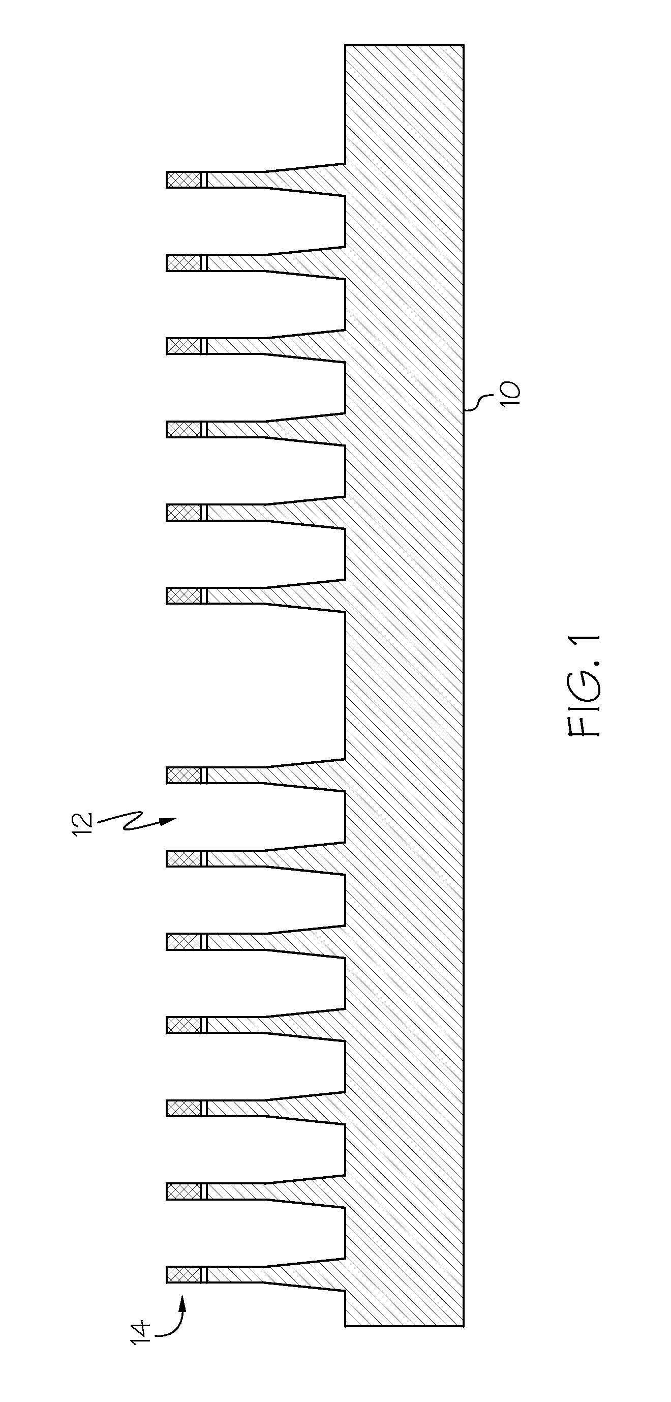
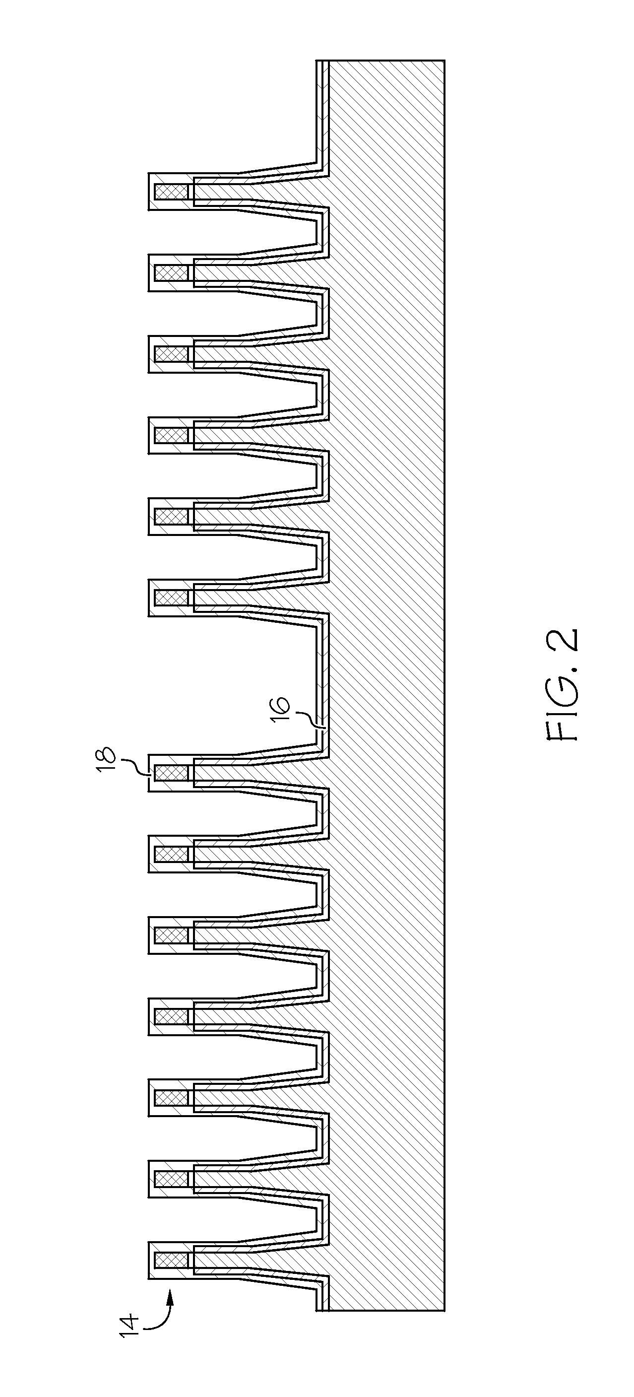
BACKGROUND[0001]1. Technical Field[0002]This invention relates generally to the field of semiconductors and, more particularly, to shallow trench isolation (STI) integration methods / schemes for improved wet etch removal rates and etch stopping.[0003]2. Related Art[0004]In current fin-based field effect transistor (FinFET) integration schemes, enhanced High Aspect Ratio Process (eHARP) is often utilized for shallow trench isolation (STI) gap fill. However, due to poor eHARP film density, severe STI-oxide recess was discovered in downstream processes. Such phenomena resulted in fin damage and poor device performance.SUMMARY OF THE INVENTION[0005]In general, aspects of the present invention relate to approaches for forming a semiconductor device such as a FinFET device through the use of multiple protective liners between bi-layers of refill. In a typical embodiment, a set of trenches will be etched in a substrate (e.g., silicon (Si). A shallow trench isolation (STI) layer will then be...

Claims


Application Information

Patent Timeline
Patent Type & Authority Applications(United States)
IPC IPC(8): H01L21/762
CPCH01L21/76224H01L21/02123H01L21/76229H01L29/0649H01L27/0886
Inventor SHEN, HONGLIANGNA, KYUTAEGAAN, SANDEEPTAI, HSIN-NENGTONG, WEIHUAHAN, SANG CHEOLKIMHAN, JA HYUNGHUANG, HAIGOUXIAO, CHANGYONGLIU, HUANGKIM, SEUNG YEON
Owner GLOBALFOUNDRIES US INC
Learn More