
Transparent organic light emitting display device and method for manufacturing the same

a technology of organic light and display device, which is applied in the direction of electroluminescent light source, thermoelectric device, electric lighting source, etc., can solve the problems of reducing the available space for other components of the organic light emitting display device, unable to uniformly illuminate the screen, and auxiliary electrode spa

Active Publication Date: 2014-07-03
LG DISPLAY CO LTD
View PDF1 Cites 181 Cited by
  • Summary
  • Abstract
  • Description
  • Claims
  • Application Information

AI Technical Summary

Benefits of technology

The patent describes an improved transparent organic light emitting display device with a better arrangement of auxiliary electrodes and sub pixels. The device includes a plurality of sub pixels, each with two areas of function. Auxiliary electrodes are electrically connected to at least some of the sub pixels, and in one embodiment, an auxiliary electrode is disposed between the first and second sub pixels. The device also includes a method for manufacturing it. Overall, the patent aims to improve the performance and efficiency of transparent organic light emitting display devices.

Problems solved by technology

The increased electrical resistance, in turn, causes voltage drop in some parts of the organic light emitting display device creating non-uniform luminance throughout the screen.
The amount of space used by the auxiliary electrode in the organic light emitting display device reduces the available space for other components of the organic light emitting display device.
The number of auxiliary electrodes employed in an organic light emitting display device makes it even harder to manage the space within the organic light emitting display device, which is often a critical aspect in most modern display devices.
This is especially true for transparent organic light emitting display device, because placing the auxiliary electrode(s) in the pixel area reduces the size of the emissive area and / or the transmissive area, resulting in poor luminance and / or poor transparency through the display device.

Method used


Image

  • Transparent organic light emitting display device and method for manufacturing the same
  • Transparent organic light emitting display device and method for manufacturing the same
  • Transparent organic light emitting display device and method for manufacturing the same

Examples


Embodiment Construction

[0033]Various advantages and features of the present invention and methods accomplishing thereof will become apparent from the following description of embodiments with reference to the accompanying drawings. However, the present invention is not limited to exemplary embodiment disclosed herein but will be implemented in various forms. The exemplary embodiments are provided by way of example only so that a person of ordinary skilled in the art can fully understand the disclosures of the present invention and the scope of the present invention. Therefore, the present invention will be defined only by the scope of the appended claims.

[0034]In the following description, numerous specific details are set forth, such as particular structures, components, materials, dimensions, processing steps and techniques, in order to provide an understanding of the various embodiments of the present disclosure. In other instances, well-known structures or processing steps have not been described in d...


PUM


Abstract

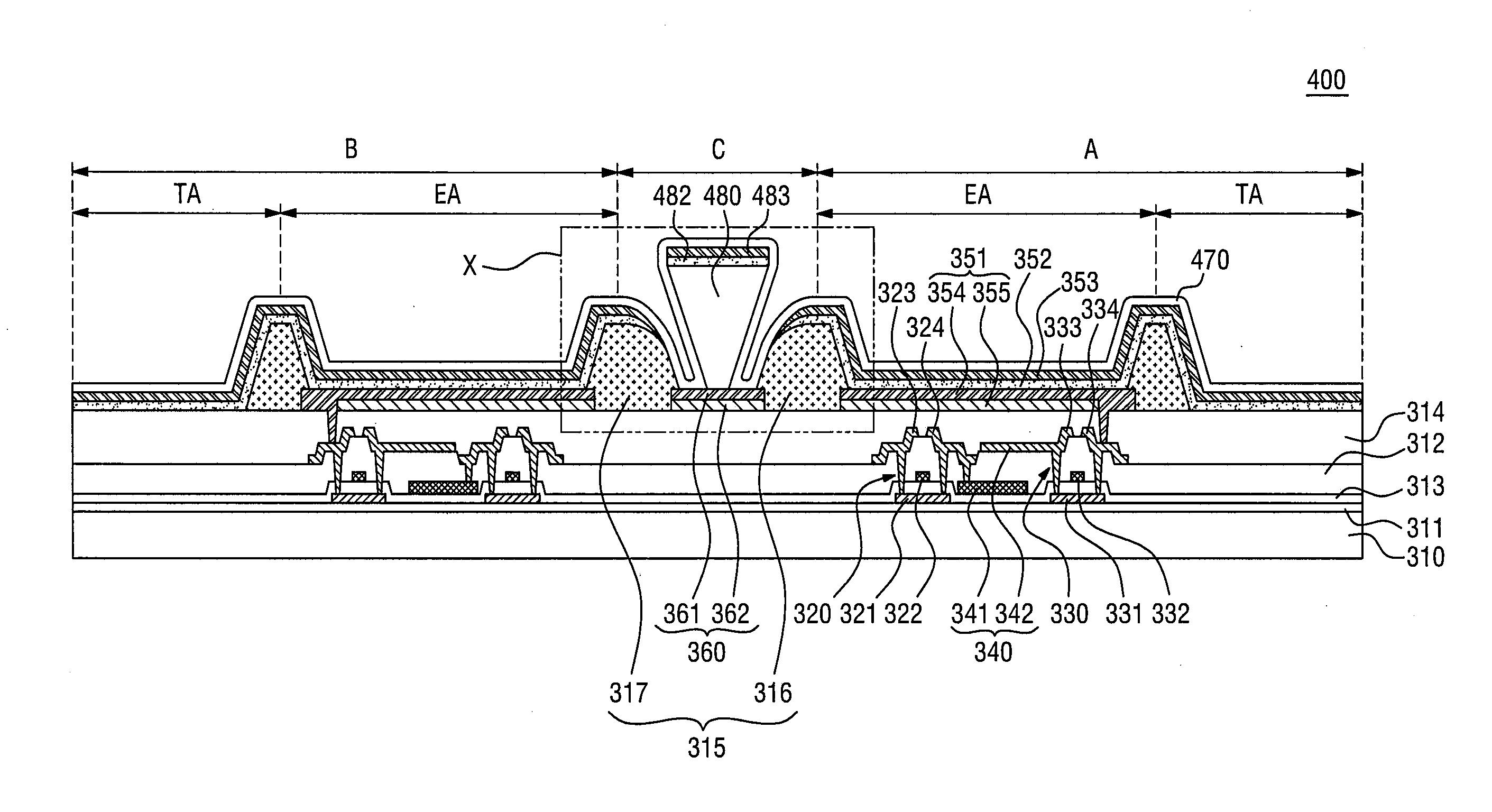
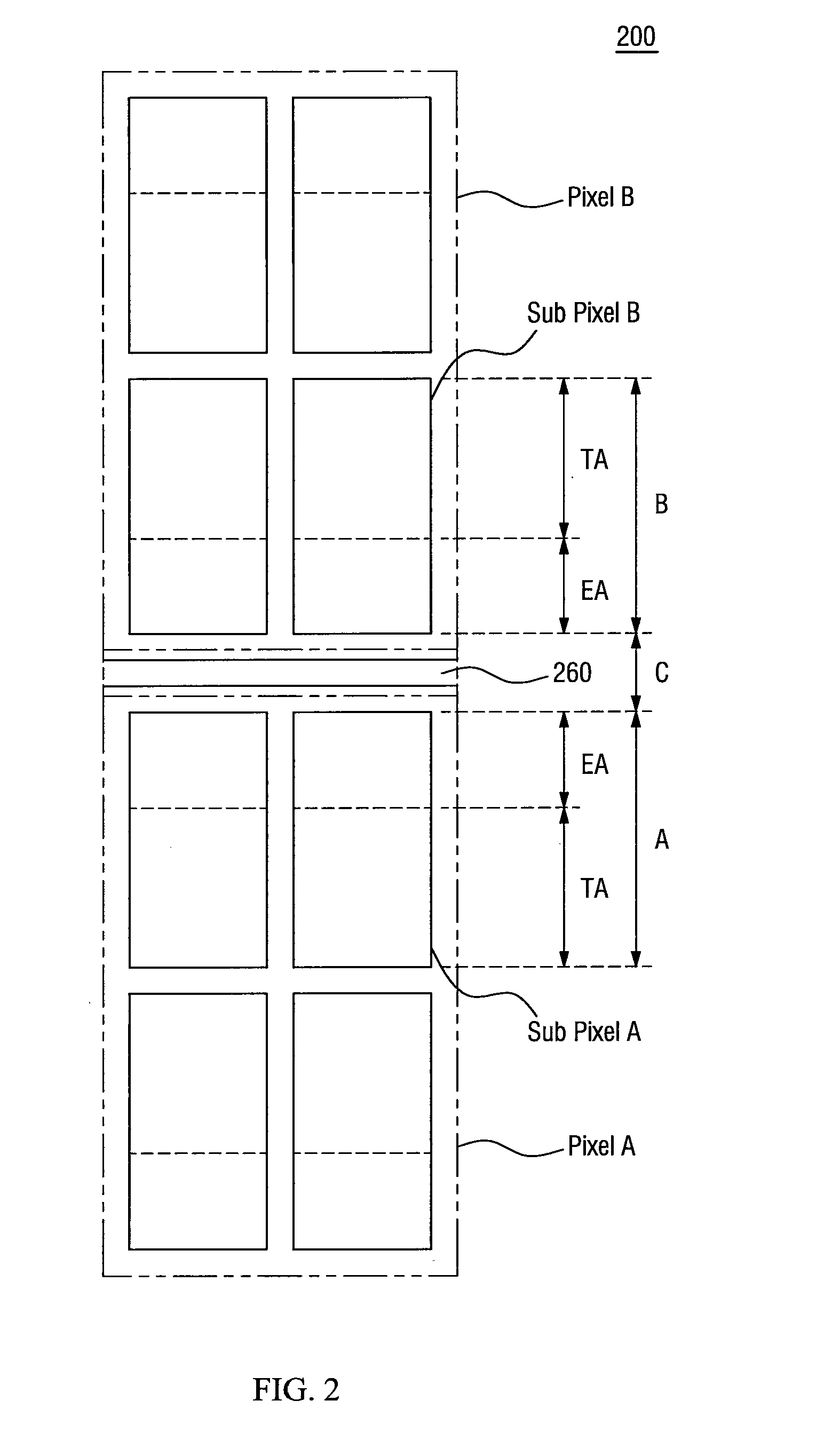
Provided are an organic light emitting display device and a method for manufacturing the same. The organic light emitting display device includes a plurality of pixels, each including a set of sub pixels. Each of the sub pixels has an emissive area for emitting light and a transmissive area for passing the external light. At least two sub pixels are symmetrically arranged on each side of an auxiliary electrode, and share the auxiliary electrode.

Description

CROSS-REFERENCE TO RELATED APPLICATIONS[0001]This application claims the priority of Korean Patent Application No. 10-2012-0155929 filed on Dec. 28, 2012, in the Korean Intellectual Property Office, the disclosure of which is incorporated herein by reference.BACKGROUND[0002]1. Field of the Invention[0003]The embodiments herein relate to a transparent organic light emitting display device and a method for manufacturing the same, and more particularly, to a transparent organic light emitting display device with an auxiliary electrode and pixel / sub pixel layouts for enhancing the image quality without sacrificing the luminance and transparency of the display device.[0004]2. Description of the Related Art[0005]An organic light emitting diode (OLED) display device, as a self-emission display device, does not require a separate light source as a liquid crystal display (LCD). Further, the OLED display device is more power efficient and has better response speed, viewing angle and contrast ...

Claims


Application Information

Patent Timeline
IPC IPC(8): H01L27/32H01L51/56
CPCH01L51/56H01L27/3237H10K59/352H10K59/353H10K59/121H10K59/122H10K59/1315H10K59/131H10K2102/3031H10K59/80522H05B33/22H10K71/00H10K50/824
Inventor PARK, SUNGHEEKIM, BINNKIM, JONGMOO
Owner LG DISPLAY CO LTD
Learn More