Color filter substrate for in-cell touch panel and manufacturing method thereof
a technology of color filter substrate and touch panel, which is applied in the field of color filter substrate for in-cell touch panel, can solve the problem of a relative long time required for completing the application
- Summary
- Abstract
- Description
- Claims
- Application Information
AI Technical Summary
Benefits of technology
Problems solved by technology
Method used
Image

Examples
Embodiment Construction
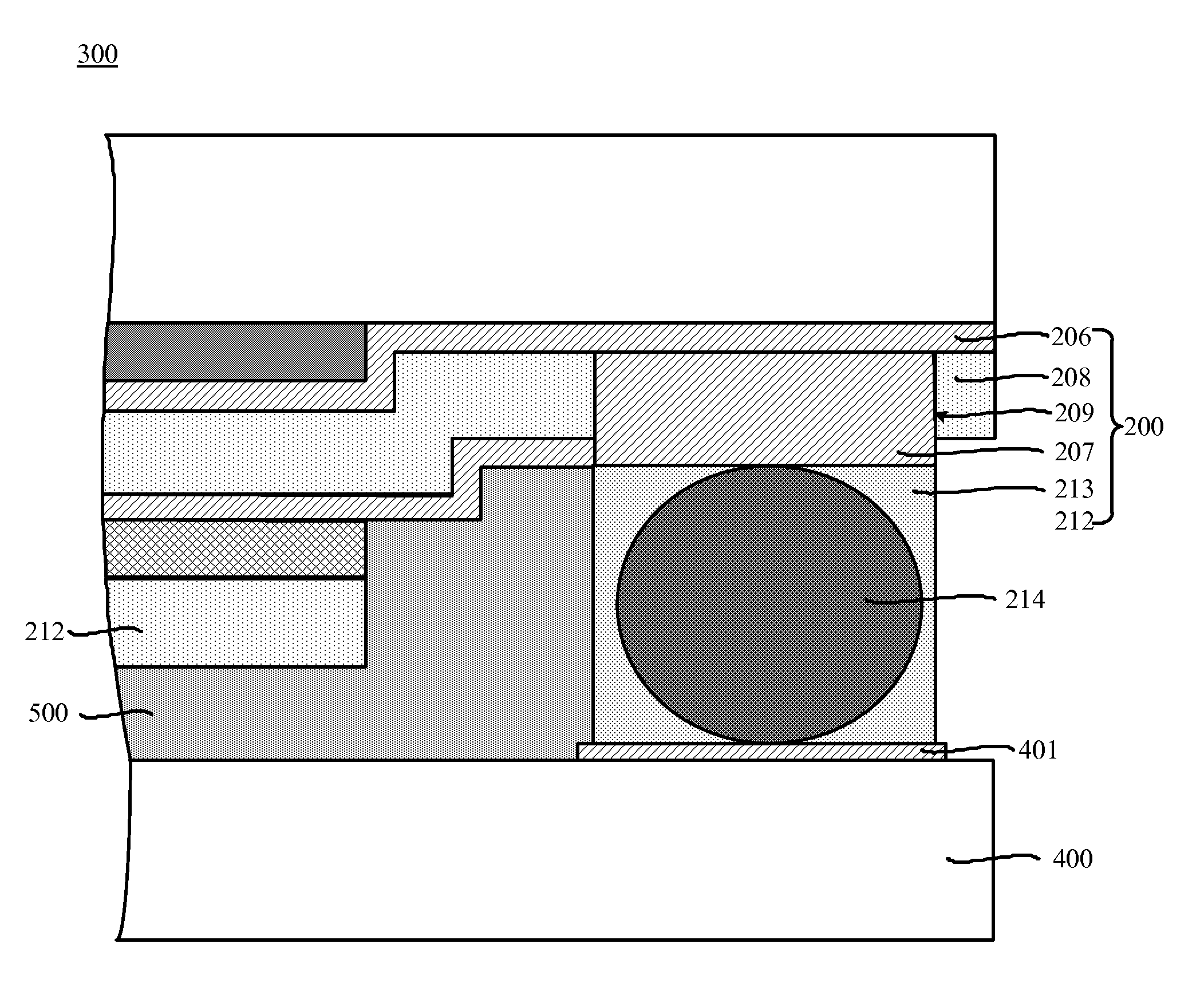
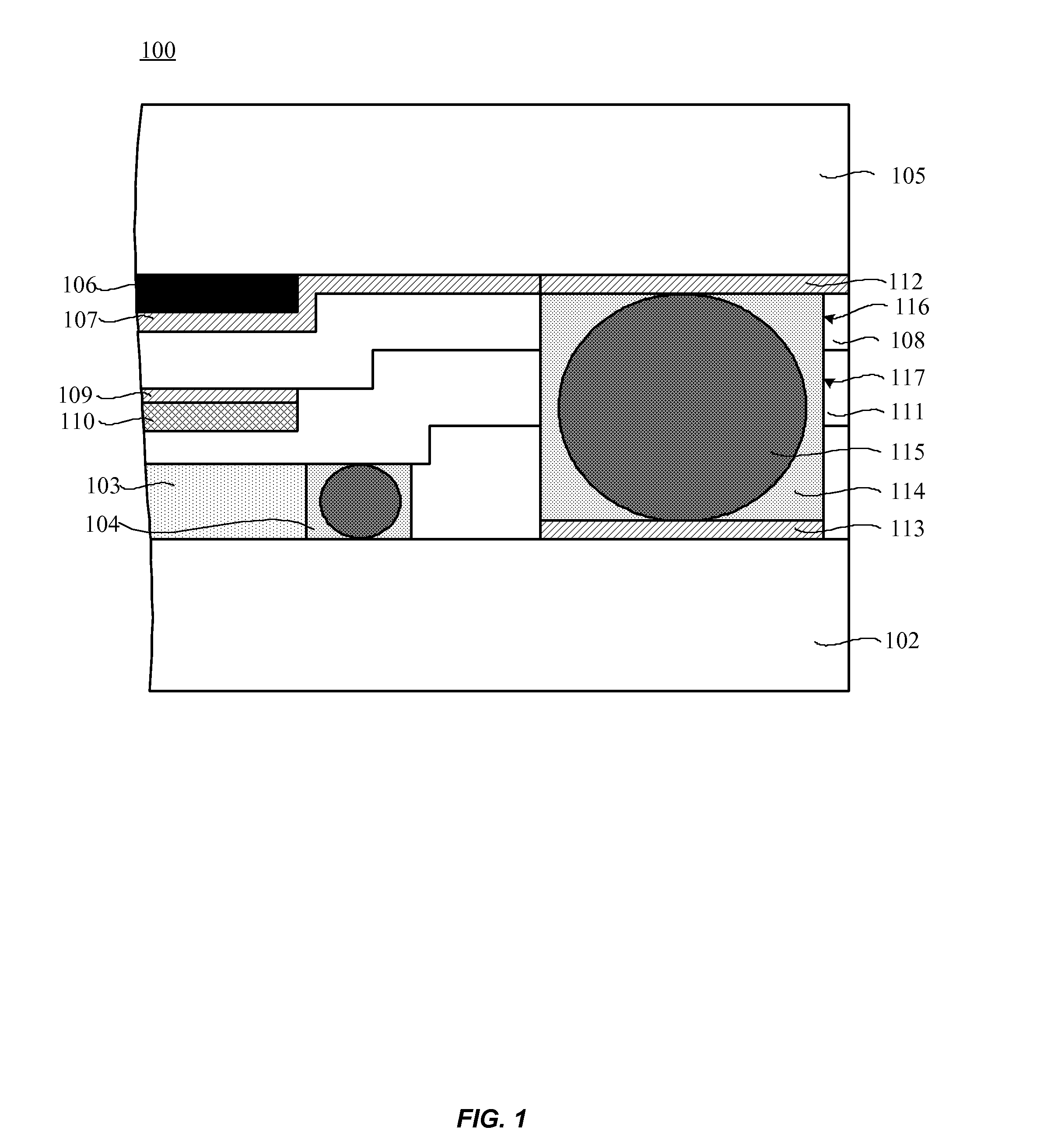
[0016]The concept of the present invention lies in providing a through hole or through slot in a first organic film layer in a non-display area of the in-cell touch color filter substrate and connecting a first metal layer and a second metal layer by a conductive pad passing through the through hole or through slot. Therefore, in the area of the conductive pad, the first metal layer and the second metal layer are arranged one above the other and uncovered by the second organic film layer. When the sealant mixed with gold ball bonds is applied on the conductive pad area, the gold ball bonds contact the conductive pads directly. The gold ball bonds contact the second metal layer without passing through holes having level differences (i.e. steps). Even if the deviation of the positions of applying the sealant mixed with gold ball bonds would not cause the case in which the gold ball bonds are unable to enter the holes precisely and hence fail to contact the conductive pads, so that the...
PUM
| Property | Measurement | Unit |
|---|---|---|
| thickness | aaaaa | aaaaa |
| thickness | aaaaa | aaaaa |
| depth | aaaaa | aaaaa |
Abstract
Description
Claims
Application Information
 - R&D
- Intellectual Property
- Life Sciences
- Materials
- Tech Scout
- Unparalleled Data Quality
- Higher Quality Content
- 60% Fewer Hallucinations
Browse by: Latest US Patents, China's latest patents, Technical Efficacy Thesaurus, Application Domain, Technology Topic, Popular Technical Reports.
© 2025 PatSnap. All rights reserved.Legal|Privacy policy|Modern Slavery Act Transparency Statement|Sitemap|About US| Contact US: help@patsnap.com