
Conductive laminate body, touch panel, and display device

a technology of touch panel and conductive laminate, which is applied in the direction of static indicating devices, instruments, synthetic resin layered products, etc., can solve the problems of delay in response speed and the speed of current transfer between the electrodes, and achieve the effect of being easy to see for users

Active Publication Date: 2014-04-10
FUJIFILM CORP
View PDF21 Cites 30 Cited by
  • Summary
  • Abstract
  • Description
  • Claims
  • Application Information

AI Technical Summary

Benefits of technology

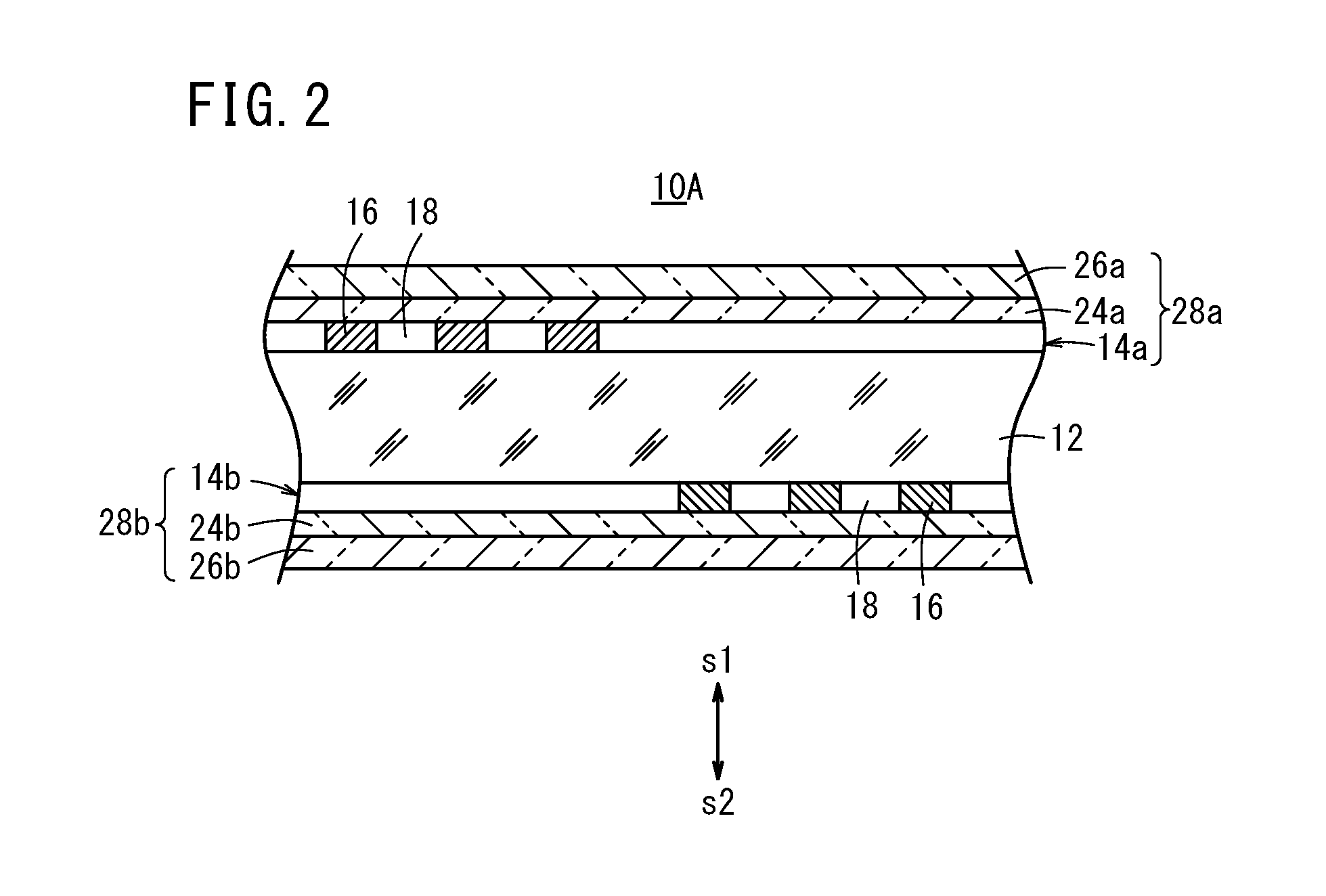
The present invention relates to a conductive laminate body, a touch panel, and a display device that can reduce the visibility of thin metal wires used in a mesh pattern. This is achieved by increasing the amount of light that travels in a straight line at the boundaries between the substrate and the protective layers, without scattering or interference from the thin metal wires. This decreases the contrast in optical density caused by the thin metal wires and reduces the generation of moiré phenomena, making the device more visually appealing.

Problems solved by technology

As a result, a problem arises in that the transmission speed of current between the electrodes becomes slower, such that the time (i.e., response speed) required to detect the contact position after the touch panel has been touched is delayed.

Method used


Image

  • Conductive laminate body, touch panel, and display device
  • Conductive laminate body, touch panel, and display device
  • Conductive laminate body, touch panel, and display device

Examples


##ventive example 1

Inventive Example 1

[0213]A conductive laminate body 10 according to the first inventive example was manufactured in 20 types using polychlorotrifluoroethylene (PCTFE) with an index of refraction n1=1.42 as the first protective layer 26a. In this case, the relative index of refraction nr1 was nr1=(1.42 / 1.64)=0.86.

##ventive example 2

Inventive Example 2

[0214]A conductive laminate body 10 according to the second inventive example was manufactured in 20 types using polymethyl methacrylate (PMMA) with an index of refraction n1=1.50 as the first protective layer 26a. In this case, the relative index of refraction nr1 was nr1=(1.50 / 1.64)=0.91.

##ventive example 3

Inventive Example 3

[0215]A conductive laminate body 10 according to the third inventive example was manufactured in 20 types using polystyrene (PS) with an index of refraction n1=1.60 as the first protective layer 26a. In this case, the relative index of refraction nr1 was nr1=(1.60 / 1.64)=0.97.


PUM

PropertyMeasurementUnit
Timeaaaaaaaaaa
Angleaaaaaaaaaa
Angleaaaaaaaaaa

Abstract

This present invention pertains to: a conductive laminate body, a touch panel, and a display device. In the present invention, the relative refractive index of a substrate with respect to a first protective sheet, and / or the relative refractive index of the substrate with respect to a second protective sheet is 0.86-1.15. The relative refractive index of a first substrate with respect to the first protective sheet, and / or the relative refractive index of a second substrate with respect to the second protective sheet is 0.86-1.15.

Description

CROSS-REFERENCE TO RELATED APPLICATIONS AND PRIORITY CLAIM[0001]This application is a Continuation of International Application No. PCT / JP2012 / 067621 filed on Jul. 10, 2012, which was published under PCT Article 21(2) in Japanese, which is based upon and claims the benefit of priority from Japanese Patent Application No. 2011-152648 filed on Jul. 11, 2011, the contents all of which are incorporated herein by reference.TECHNICAL FIELD[0002]The present invention relates to a conductive laminate body, a touch panel, and a display device.BACKGROUND ART[0003]Recently, electronic devices that incorporate touch panels therein have been spreading widely. Touch panels are mounted in many devices including small screen, such as portable phones, PDAs (Personal Digital Assistants), or the like. In the future, it can be envisaged sufficiently that such touch panels will be incorporated into equipment having large sized screens that serve as PC (Personal Computer) displays or the like.[0004]In th...

Claims


Application Information

Patent Timeline
IPC IPC(8): H05K1/02G06F3/041
CPCG06F3/041H05K1/0213B32B7/12B32B15/02B32B15/08B32B27/302B32B27/304B32B27/36B32B2307/20B32B2307/202B32B2307/208B32B2307/412G02B5/1814G06F3/0445G06F3/0446G06F2203/04103G06F2203/04112G09G2320/0233G09G2320/0653G09G2320/103G09G2320/0626
Inventor IWAMI, KAZUCHIKA
Owner FUJIFILM CORP
Learn More