Field device and method of operating high voltage semiconductor device applied with the same
a field device and high voltage technology, applied in the field of field devices and methods of operating high voltage (hv) semiconductor devices, can solve the problems of failure of hv-well isolation, limited maximum operating voltage, and failure of mosfets under high voltage operation, so as to increase the cost and the effect of device area, the threshold voltage (vth) of the field device is effectively improved
- Summary
- Abstract
- Description
- Claims
- Application Information
AI Technical Summary
Benefits of technology
Problems solved by technology
Method used
Image


Examples
first embodiment
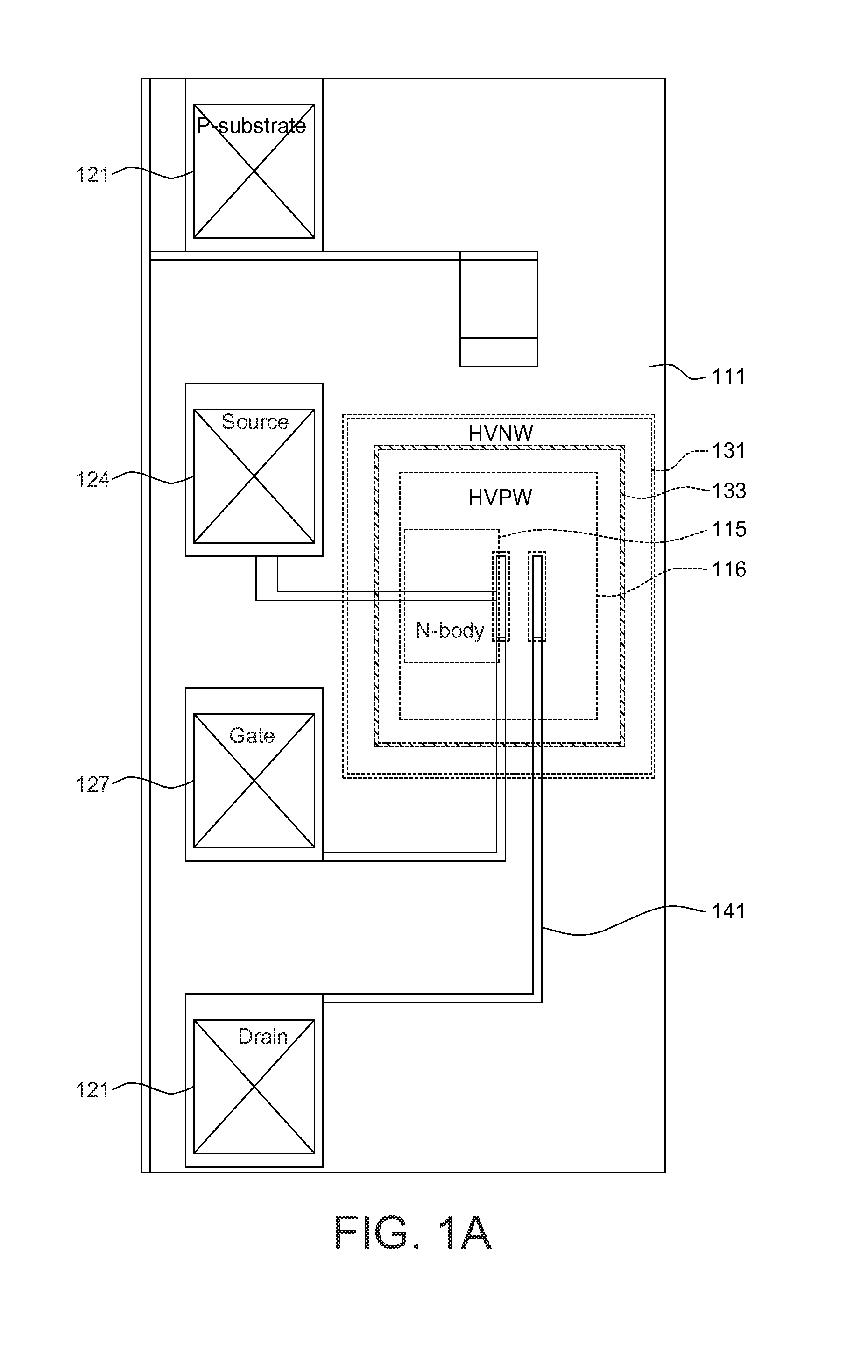
[0018]FIG. 1A is a top view of a high voltage metal-oxide-semiconductor (HVMOS) having a field device according to the first embodiment of the present disclosure. FIG. 1B is a cross-sectional view of the HVMOS and the field device corresponding to FIG. 1A according to the first embodiment of the present disclosure. Please refer to FIG. 1A and FIG. 1B. HVMOS 1 includes a P-substrate 111, the N+ Buried Layers (NBL) 112 formed within the P-substrate 111, P-wells (PW) 113, a high voltage N-well (HVNW) 114 and 131, a high voltage P-well (HVPW) 115, a N-body 116, the P+ regions 121-122 and 123, a N+ region 124 and the insulations 126. The N+ Buried Layer (NBL) 112 provides isolation functionality. The HVPW 115 is positioned between the HVNW 114 and HVNW 131. The P+ region 121 is formed within the PW 113 and electrically connected to the P-substrate 111, and the N+ region 124 is formed within the N-body 116 as a source of the HVMOS. One insulation 126 (such as oxide) are formed above the P...
second embodiment
[0024]FIG. 2A is a top view of a high voltage metal-oxide-semiconductor (HVMOS) having a field device according to the second embodiment of the present disclosure. FIG. 2B is a cross-sectional view of the HVMOS and the field device corresponding to FIG. 2A according to the second embodiment of the present disclosure. The components of the following embodiments (such as in FIG. 2A and FIG. 2B) identical or similar to the components of FIG. 1A and FIG. 1B of the first embodiment retain the same or similar reference numerals, and the details are not redundantly described.
[0025]In the field device 23 of the second embodiment, the conductive body 233 is disposed under the conductive line 141, and further electrically connected to an external voltage source for applying a fixed voltage bias to the conductive body 233. Fabrication of the conductive body 233 could also be adopted in the current manufacturing process, and no extra cost and device area are required.
[0026]In the second embodim...
third embodiment
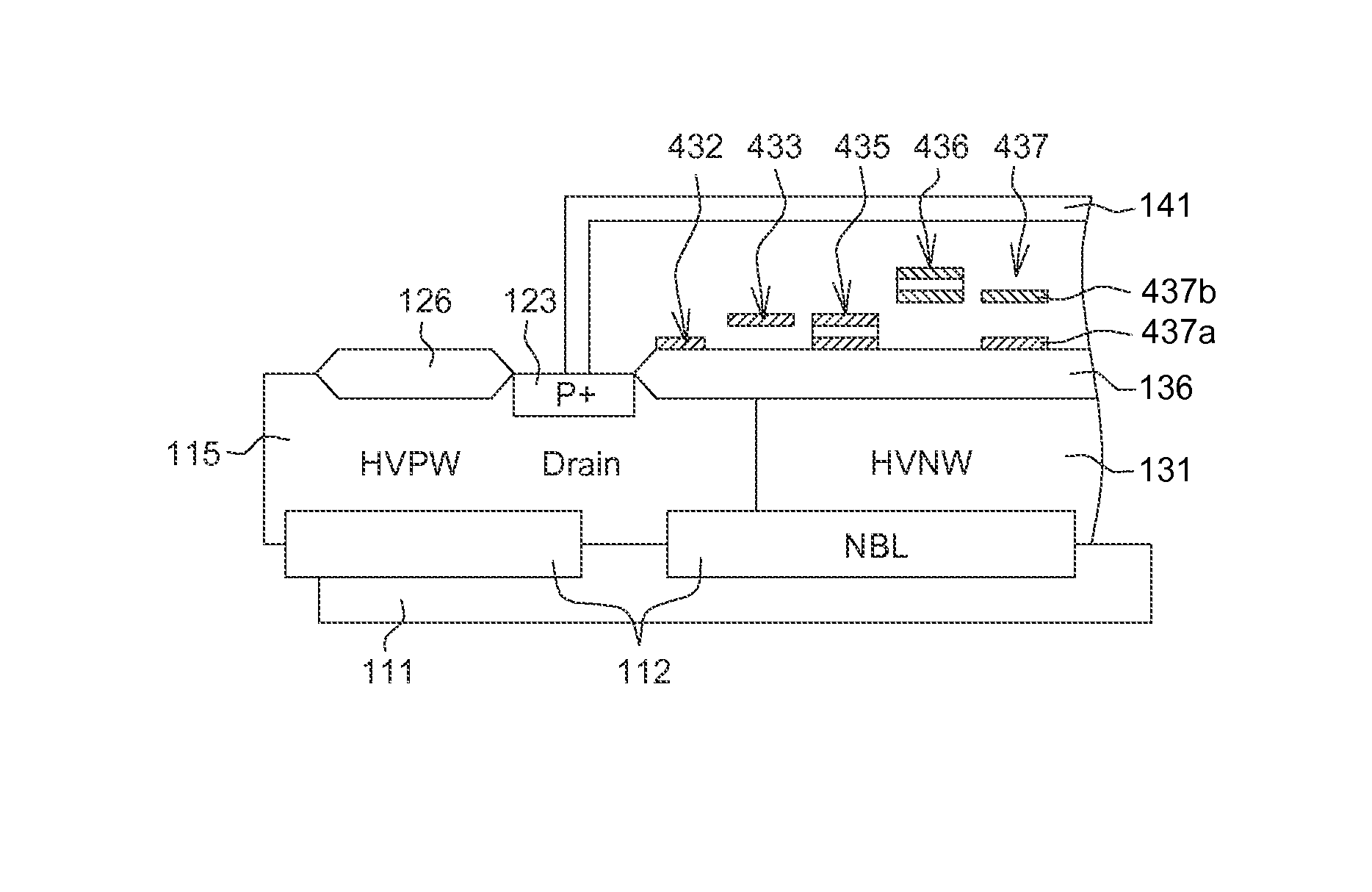
[0027]FIG. 3 is a cross-sectional view of a field device according to the third embodiment of the present disclosure. The components of FIG. 3 identical or similar to the components of FIG. 1A-FIG. 2B of the first and second embodiments retain the same or similar reference numerals, and the details are not redundantly described.
[0028]In the third embodiment, the conductive body 333 of the field device 33 is disposed between the first well (e.g. HVNW 131) and the conductive line 141, and the field device 33 further comprises a second doping region 332 formed in the first well (e.g. HVNW 131) for interrupting continuity of the first well. The second doping region 332 and the first well have same dosage type (e.g. the second conductive type), and the doping concentration of the second doping region 332 is larger than the doping concentration of the first well, and the second doping region 332 is electrically connected to the conductive body 333. In one embodiment, the second doping reg...
PUM
 Abstract
Description
Claims
Application Information
 - R&D
- Intellectual Property
- Life Sciences
- Materials
- Tech Scout
- Unparalleled Data Quality
- Higher Quality Content
- 60% Fewer Hallucinations
Browse by: Latest US Patents, China's latest patents, Technical Efficacy Thesaurus, Application Domain, Technology Topic, Popular Technical Reports.
© 2025 PatSnap. All rights reserved.Legal|Privacy policy|Modern Slavery Act Transparency Statement|Sitemap|About US| Contact US: help@patsnap.com