
Iii-nitride enhancement mode transistors with tunable and high gate-source voltage rating

a technology of iii-nitride and enhancement mode, which is applied in the field of gallium nitride fets in semiconductor devices, can solve the problems of gate dielectric breakdown of enhancement mode gan fets with insulated gates, undetectable gate leakage current,

Active Publication Date: 2014-02-13
TEXAS INSTR INC
View PDF4 Cites 41 Cited by
  • Summary
  • Abstract
  • Description
  • Claims
  • Application Information

AI Technical Summary

Benefits of technology

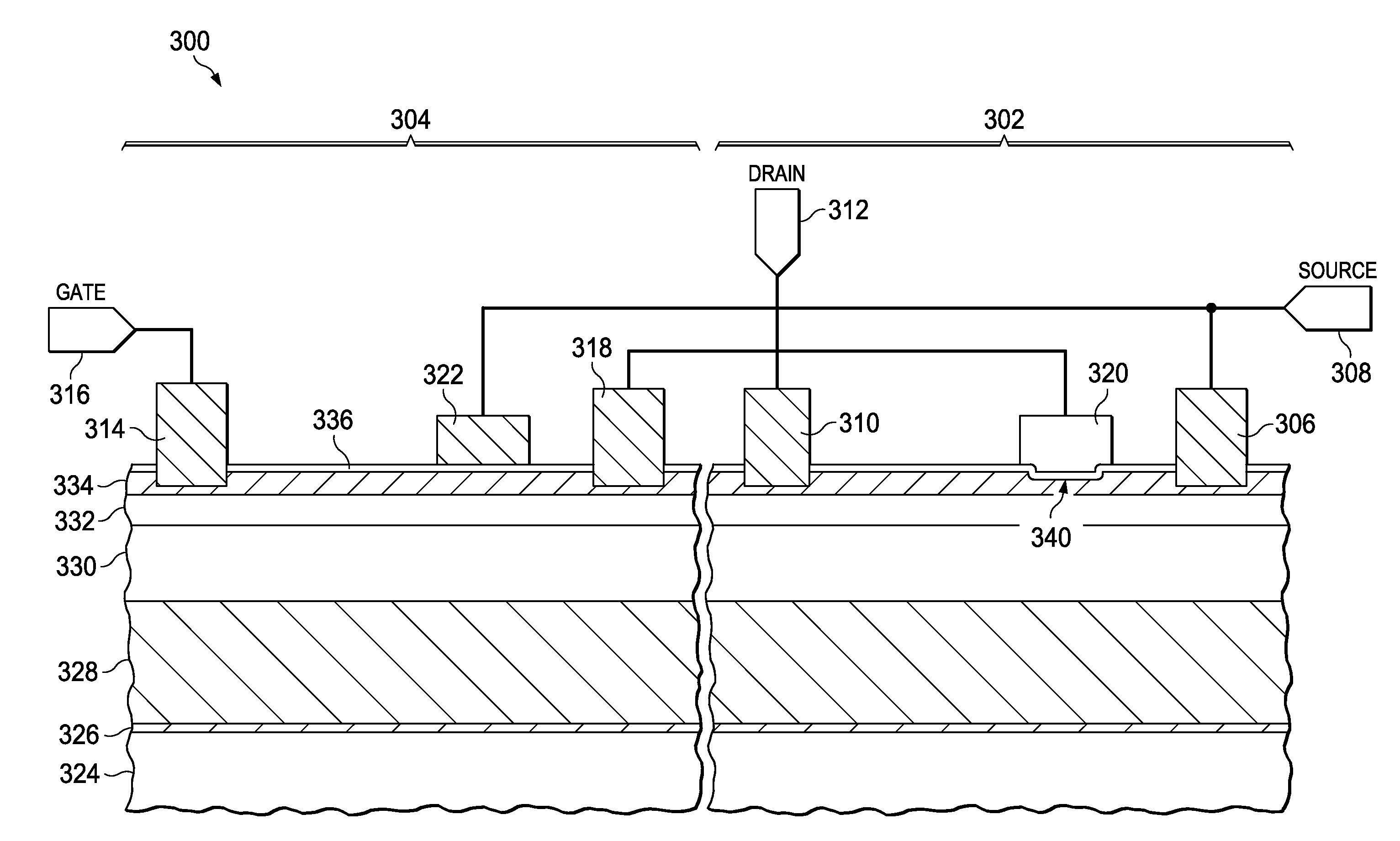
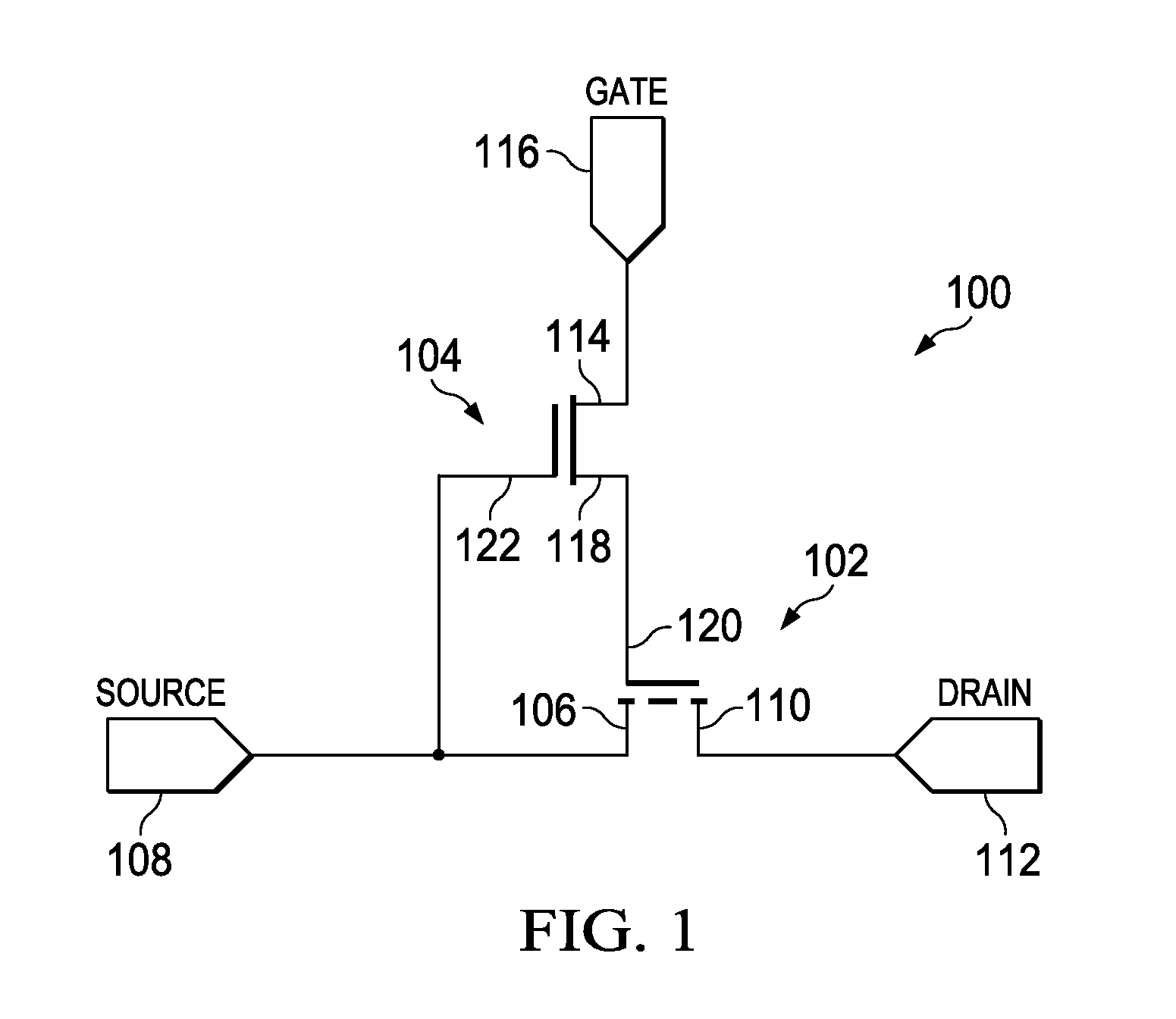
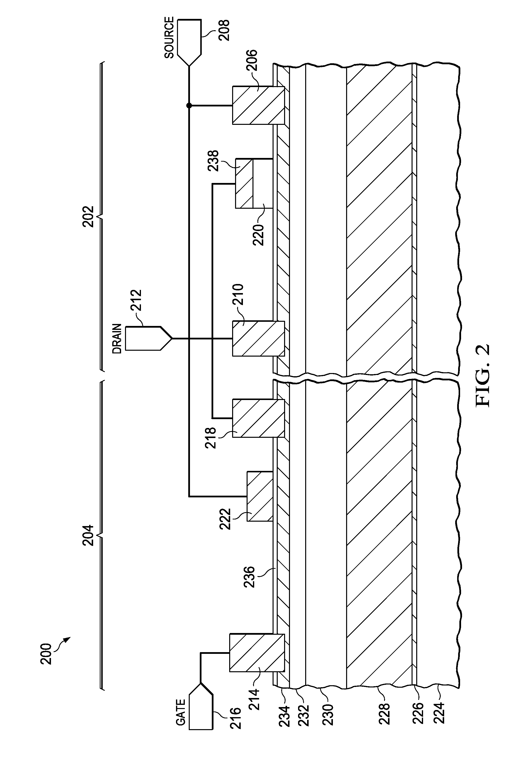
The patent describes a way to control the operation of a semiconductor device by applying different gate bias to it. A low gate bias is used initially to minimize voltage drop and maintain the desired operation. When a higher gate bias is applied, the device goes into a pinch-off mode to maintain the desired operation. This results in a more efficient and controlled operation of the semiconductor device.

Problems solved by technology

However, enhancement mode GaN FETs with semiconductor gates are undesirably susceptible to excessive gate leakage current when the gates are overbiased.
Similarly, enhancement mode GaN FETs with insulated gates are susceptible to gate dielectric breakdown when the gates are overbiased.

Method used


Image

  • Iii-nitride enhancement mode transistors with tunable and high gate-source voltage rating
  • Iii-nitride enhancement mode transistors with tunable and high gate-source voltage rating
  • Iii-nitride enhancement mode transistors with tunable and high gate-source voltage rating

Examples


Embodiment Construction

[0009]The following co-pending patent applications are related and hereby incorporated by reference:

[0010]U.S. patent application Ser. No. 12 / ______ (TI-71206 filed simultaneously with this application, entitled “AVALANCHE ENERGY HANDLING CAPABLE III-NITRIDE TRANSISTORS;”

[0011]U.S. patent application Ser. No. 12 / ______ (TI-71209 filed simultaneously with this application, entitled “III-NITRIDE TRANSISTOR LAYOUT;”

[0012]U.S. patent application Ser. No. 12 / ______ (TI-71492 filed simultaneously with this application, entitled “LAYER TRANSFER OF SI100 ON TO III-NITRIDE MATERIAL FOR HETEROGENOUS INTEGRATION;”

[0013]U.S. patent application Ser. No. 12 / ______ (TI-72417 filed simultaneously with this application, entitled “RESURF III-NITRIDE HEMTS;”

[0014]U.S. patent application Ser. No. 12 / ______ (TI-72418 filed simultaneously with this application, entitled “METHOD TO FORM STEPPED DIELECTRIC FOR FIELD PLATE FORMATION;” and

[0015]U.S. patent application Ser. No. 12 / ______ (TI-72605 filed simul...


PUM


Abstract

A semiconductor device includes an enhancement mode GaN FET with a depletion mode GaN FET electrically coupled in series between a gate node of the enhancement mode GaN FET and a gate terminal of the semiconductor device. A gate node of the depletion mode GaN FET is electrically coupled to a source node of the enhancement mode GaN FET. A source node of said enhancement mode GaN FET is electrically coupled to a source terminal of the semiconductor device, a drain node of the enhancement mode GaN FET is electrically coupled to a drain terminal of said semiconductor device, and a drain node of the depletion mode GaN FET is electrically coupled to a gate terminal of the semiconductor device.

Description

CROSS-REFERENCE TO RELATED APPLICATIONS[0001]This application claims the benefit of priority under U.S.C. §119(e) of U.S. Provisional Application 61 / 681,298 (Texas Instruments docket number TI-71208PS, filed Aug. 9, 2012, entitled “III-NITRIDE ENHANCEMENT MODE TRANSISTORS WITH TUNABLE AND HIGH GATE-SOURCE VOLTAGE RATING.”FIELD OF THE INVENTION[0002]This invention relates to the field of semiconductor devices. More particularly, this invention relates to gallium nitride FETs in semiconductor devices.BACKGROUND OF THE INVENTION[0003]Field effect transistors (FETs) made of III-N materials such as GaN exhibit desirable properties for power switches, such as high bandgaps and high thermal conductivity compared to silicon FETs. However, enhancement mode GaN FETs with semiconductor gates are undesirably susceptible to excessive gate leakage current when the gates are overbiased. Similarly, enhancement mode GaN FETs with insulated gates are susceptible to gate dielectric breakdown when the ...

Claims


Application Information

Patent Timeline
Patent Type & Authority Applications(United States)
IPC IPC(8): H01L29/66H01L29/20
CPCH01L29/7786H01L29/1066H01L27/0605H01L29/42316H01L29/66477H01L21/8258H01L29/2003H01L29/20H01L29/66H01L21/8252H01L29/4236
Inventor PENDHARKAR, SAMEERTIPIRNENI, NAVEEN
Owner TEXAS INSTR INC
Learn More