Semiconductor device and driving method thereof
a technology of semiconductor devices and driving methods, applied in information storage, static storage, digital storage, etc., can solve problems such as malfunctions in writing/reading data to/from nonvolatile memory, and achieve the effect of reducing the power consumption of semiconductor devices
- Summary
- Abstract
- Description
- Claims
- Application Information
AI Technical Summary
Benefits of technology
Problems solved by technology
Method used
Image

Examples
embodiment 1
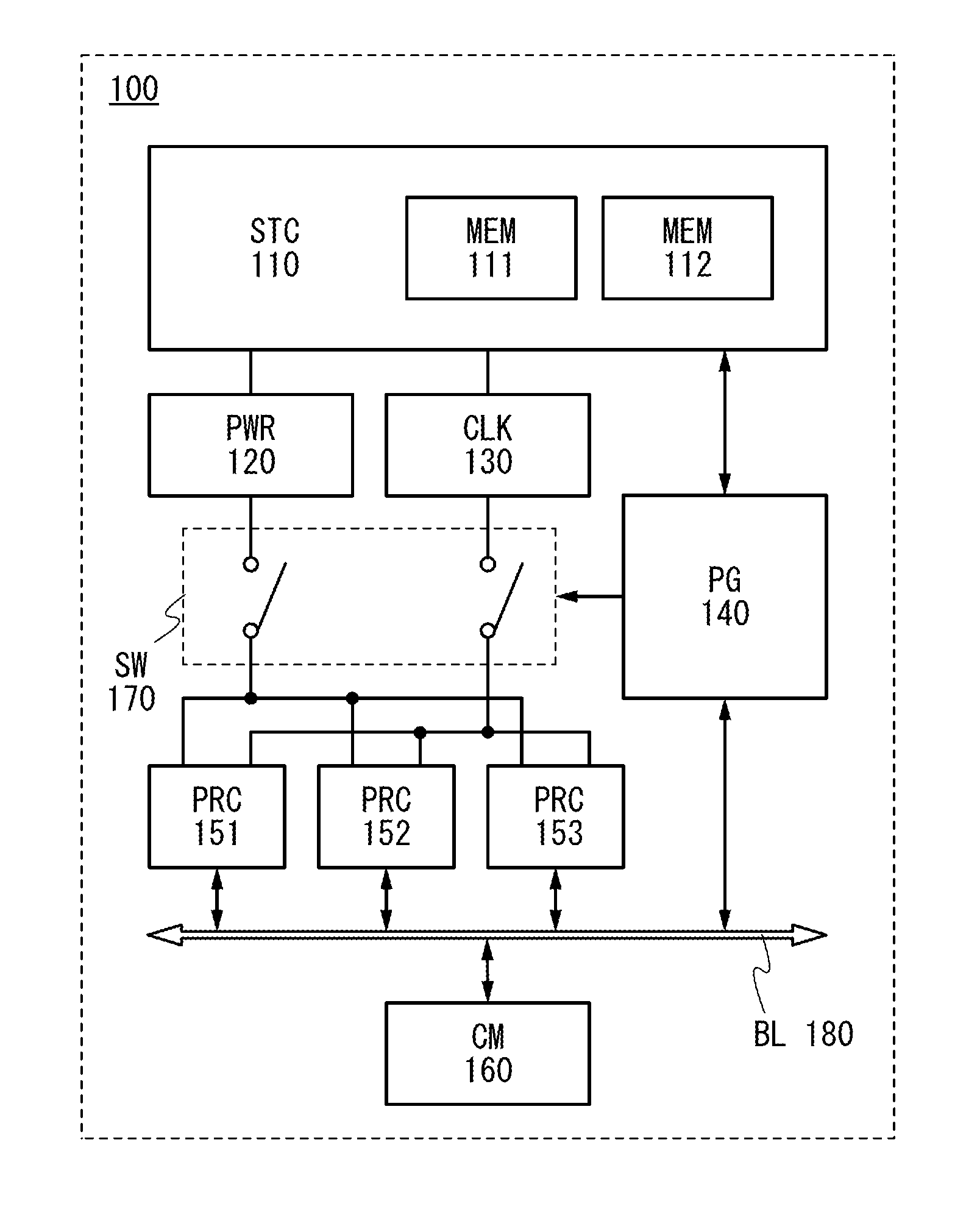
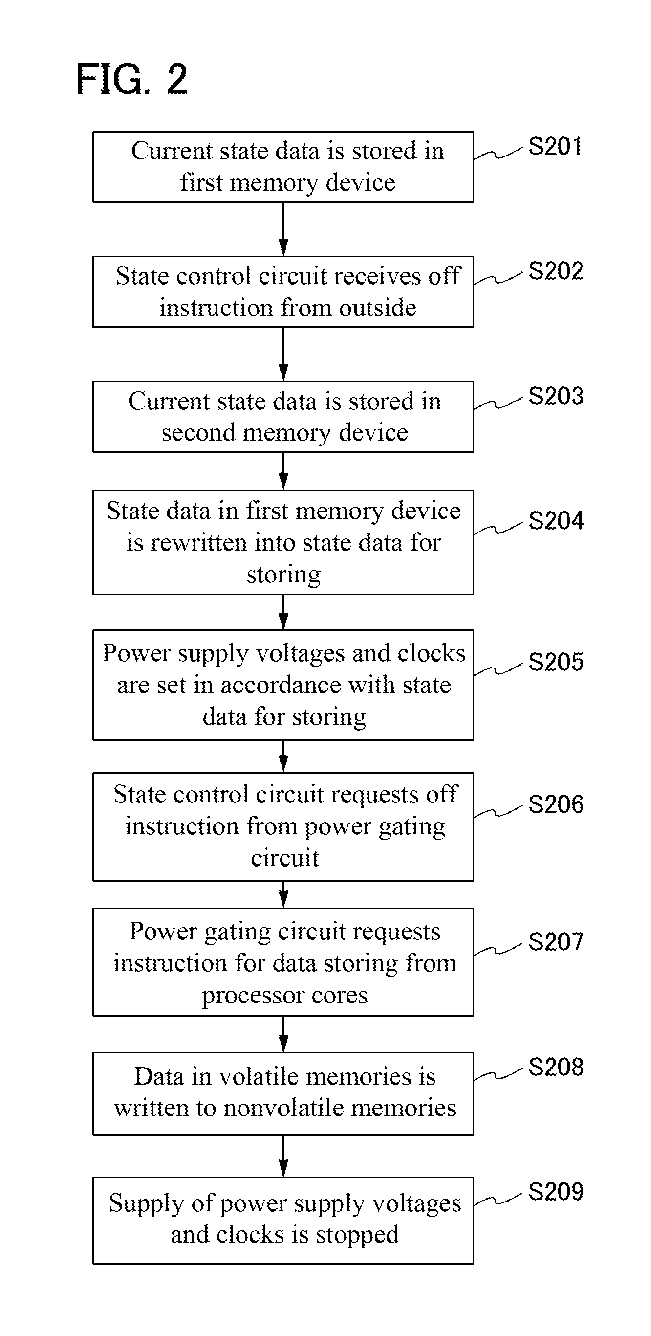
[0047]In this embodiment, a structure and a driving method of a semiconductor device of one embodiment of the present invention will be described.
[0048]As a measure to reduce power consumption of a processor, there is a method in which data in a volatile memory device such as a register or a cache memory included in the processor is stored in a nonvolatile memory device formed in the periphery of the volatile memory device, and supply of power supply voltage to a signal processing circuit including the register or the cache memory is temporarily stopped. Since supply of the power supply voltage to the signal processing circuit is stopped in a period during which data is not input or output, power consumption can be reduced without a significant degradation of the processing capacity of the processor.
[0049]In this specification, the term “nonvolatile” means a property of retaining stored data even when power supply is stopped, and the term “volatile” means a property of erasing store...
embodiment 2
[0106]In this embodiment, an example of a memory element including a nonvolatile memory, which can be used in the semiconductor device described in Embodiment 1, will be described.
[0107]FIG. 7 is an example of a circuit diagram of a memory element (register) including a nonvolatile memory. A memory element 700 includes a volatile memory circuit 701, a nonvolatile memory circuit 702, a switch 703, a switch 704, a logic element 706, a capacitor 707, and a selector circuit 720. The volatile memory circuit 701 holds data only in a period during which a power supply voltage is supplied. The nonvolatile memory circuit 702 includes a capacitor 708, a transistor 709, and a transistor 710.
[0108]Note that the memory element 700 may further include another circuit element such as a diode, a resistor, or an inductor, as needed.
[0109]The transistor 709 is a transistor in which a channel is formed in an oxide semiconductor layer. In FIG. 7, “OS” is written beside a transistor in order to indicate...
embodiment 3
[0137]In this embodiment, an example of a memory device that can be used for any of the nonvolatile memories described in Embodiments 1 and 2 and includes a transistor including an oxide semiconductor will be described with reference to drawings.
[0138]FIGS. 9A to 9C are each a cross-sectional view of an example of the nonvolatile memory circuit 702 in Embodiment 2.
[0139]The nonvolatile memory circuit 702 illustrated in FIG. 9A includes, in the lower portion, the transistor 710 in which a first semiconductor material (a substrate 3000) is used for a channel formation region, and includes, in the upper portion, the transistor 709 in which a second semiconductor material 3210 is used for a channel formation region and the capacitor 708. One electrode of the capacitor 708 is a layer that can be formed through the same steps as a gate electrode 3260 of the transistor 709, the other electrode thereof also functions as a source electrode or drain electrode 3240 of the transistor 709, and a...
PUM
 Abstract
Description
Claims
Application Information
 - R&D
- Intellectual Property
- Life Sciences
- Materials
- Tech Scout
- Unparalleled Data Quality
- Higher Quality Content
- 60% Fewer Hallucinations
Browse by: Latest US Patents, China's latest patents, Technical Efficacy Thesaurus, Application Domain, Technology Topic, Popular Technical Reports.
© 2025 PatSnap. All rights reserved.Legal|Privacy policy|Modern Slavery Act Transparency Statement|Sitemap|About US| Contact US: help@patsnap.com