
Method and system for high speed and low memory footprint static timing analysis

a static timing analysis and memory footprint technology, applied in the field of statistical timing analysis, can solve problems such as crosstalk that complicate the timing analysis of a design, and achieve the effects of less memory, less memory, and faster solution of the design

Active Publication Date: 2013-11-07
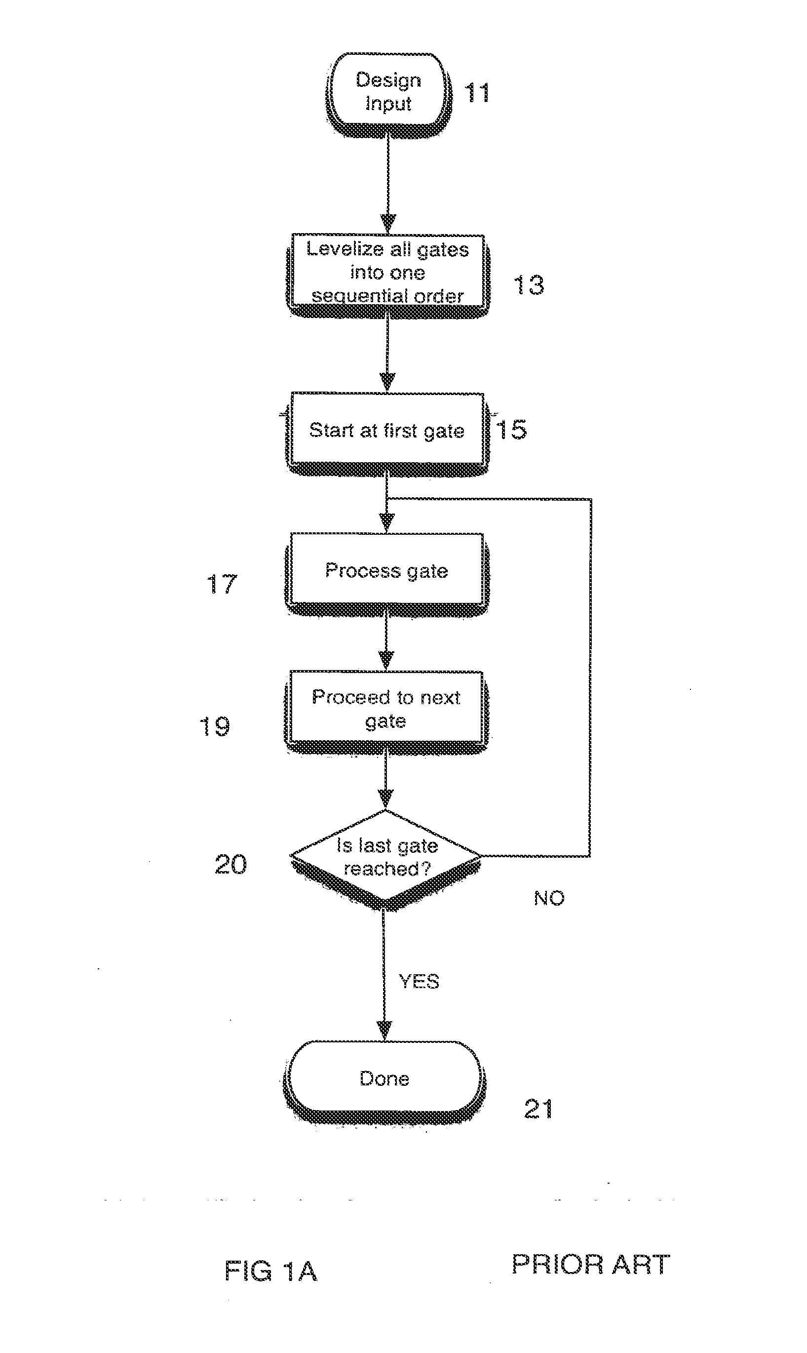
SYNOPSYS INC
View PDF0 Cites 0 Cited by
  • Summary
  • Abstract
  • Description
  • Claims
  • Application Information

AI Technical Summary

Benefits of technology

This approach enables high-speed static timing analysis with a low memory footprint, reducing hardware costs and analysis time, making it feasible to analyze large designs like SoC designs efficiently on inexpensive hardware.

Problems solved by technology

Crosstalk complicates a timing analysis of a design because crosstalk creates an even greater number of dependencies.

Method used


Image

  • Method and system for high speed and low memory footprint static timing analysis
  • Method and system for high speed and low memory footprint static timing analysis
  • Method and system for high speed and low memory footprint static timing analysis

Examples


Embodiment Construction

[0019]The inventive method and system can be further appreciated and understood by means of the figures accompanying the specification.

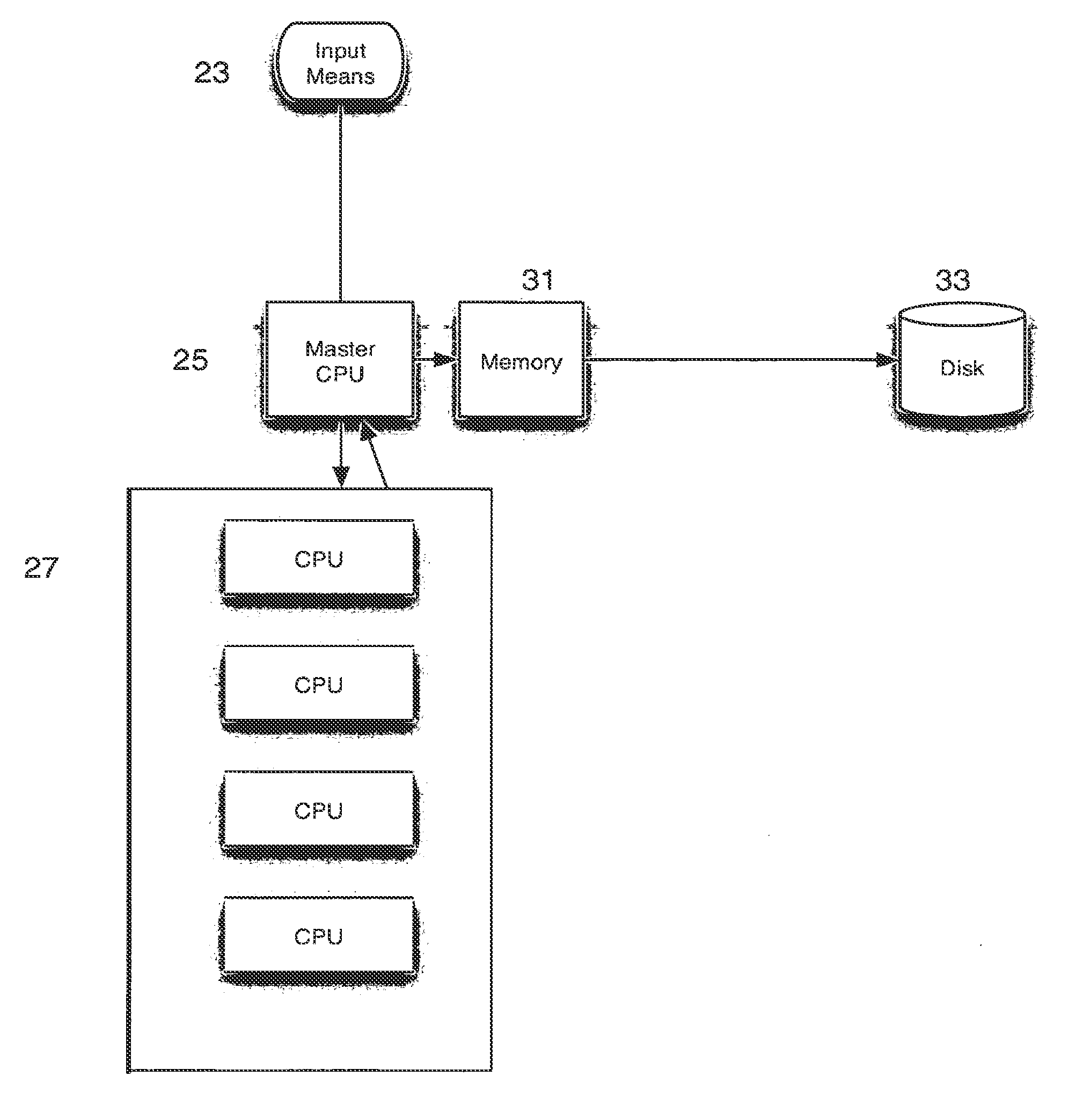
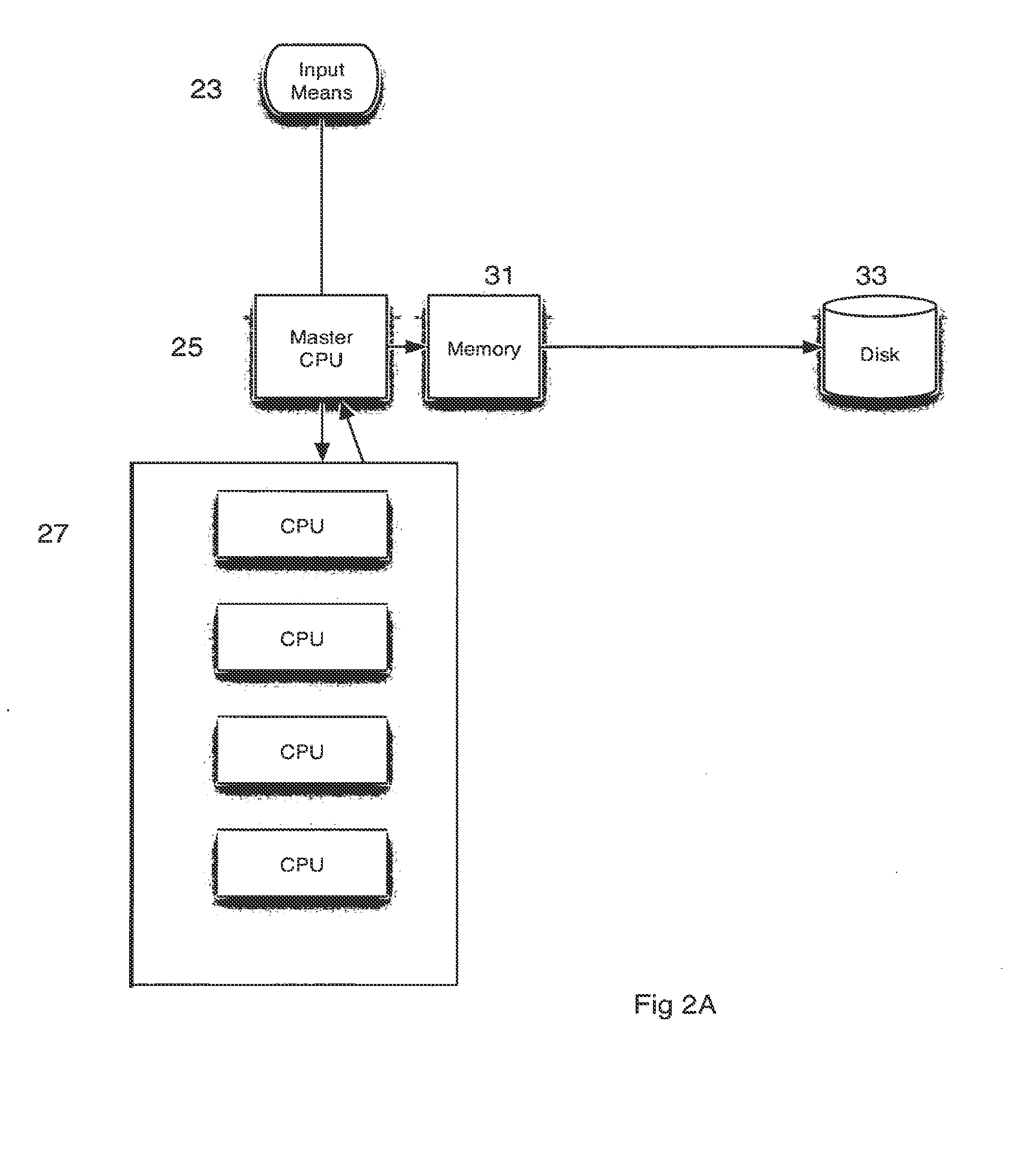
[0020]The invention provides a method of multi-threading analysis of a digital circuit design, said method including partitioning the design under analysis into a set of levels. A level may be understood as a set of gates not interdependent either before or after each other. From the master CPU, gates are sent to for solution to additional CPUs. The gates or tasks are solved independently, and the master CPU receives solutions from the dependent CPUs. When the entire level has been solved, the master CPU saves the solutions set for the level, and sends the level solution from random access memory (RAM) to a disk for storage. Solution of the next level then commences, and the process is repeated until the entire set of levels comprising the design has been solved.

[0021]Referring to FIG. 2A, a system according to the invention includes an input means f...


PUM


Abstract

The invention provides a method and system for performing Static Timing Analysis on SoC (System on a Chip) designs. The invention solves a longstanding problem with timing analysis of designs, namely, the ability to multi-thread the design under analysis. The invention provides for slicing a design into levels, further decomposing each level into gates, and the multi-threaded processing of gates so that the solution of large design analysis is generated significantly faster than current approaches. Further, the invention provides that only one level exists in the RAM at any time. Once the arrival time on the level is computed, the data is saved to disk immediately. Because the memory footprint is sub-linear to the size of the design, entire system-on-a chip designs may be run on inexpensive, off-the-shelf hardware.

Description

RELATED APPLICATIONS [0001]This application claims priority from U.S. provisional application 60 / 931,367 of the same title, filed May 22, 2007, the entirety of which is incorporated by reference as if fully set forth herein.Government Funding[0002]N / AFIELD OF USE [0003]The invention relates to statistical timing analysis, and more particularly to timing analysis of large designs, including “System-on-a-Chip” (SoC) designs.BACKGROUND [0004]A digital circuit can be represented as a set of interconnected logic gates. Static Timing Analysis (STA) is a method of computing the expected timing of a digital circuit without requiring expensive simulation. To perform static timing analysis, the arrival time at all the primary inputs are first annotated. Then the arrival time is propagated forward by adding delays along the interconnects and gates. This process continues until all primary outputs are reached.[0005]In current approaches, data generated during the arrival time propagation is all...

Claims


Application Information

Patent Timeline
Patent Type & Authority Applications(United States)
IPC IPC(8): G06F17/50
CPCG06F17/5068G06F30/3312G06F30/39G06F30/3315
Inventor MAOR, GUYCHANG, CHIN-WEI JIMKUKIMOTO, YUJILI, HAOBIN
Owner SYNOPSYS INC
Learn More