
Low-voltage fast-write nvsram cell

a nvsram cell, low-voltage technology, applied in static storage, digital storage, instruments, etc., can solve the problems of too high wl's program voltage of 20v in nand design, too large cell size, etc., to achieve fast and correct programing, not degraded fpga performance

Inactive Publication Date: 2013-11-07
APLUS FLASH TECH
View PDF22 Cites 16 Cited by
  • Summary
  • Abstract
  • Description
  • Claims
  • Application Information

AI Technical Summary

Benefits of technology

This patent describes a way to improve the performance of a memory called NVSRAM. The method helps to reduce the power needed to erase and program certain cells in the memory, which can save money and improve performance. Additionally, the method allows for faster and more accurate programming of certain cells without reversing the data polarity. Overall, this invention provides a novel way to improve the performance of NVSRAM and other memories.

Problems solved by technology

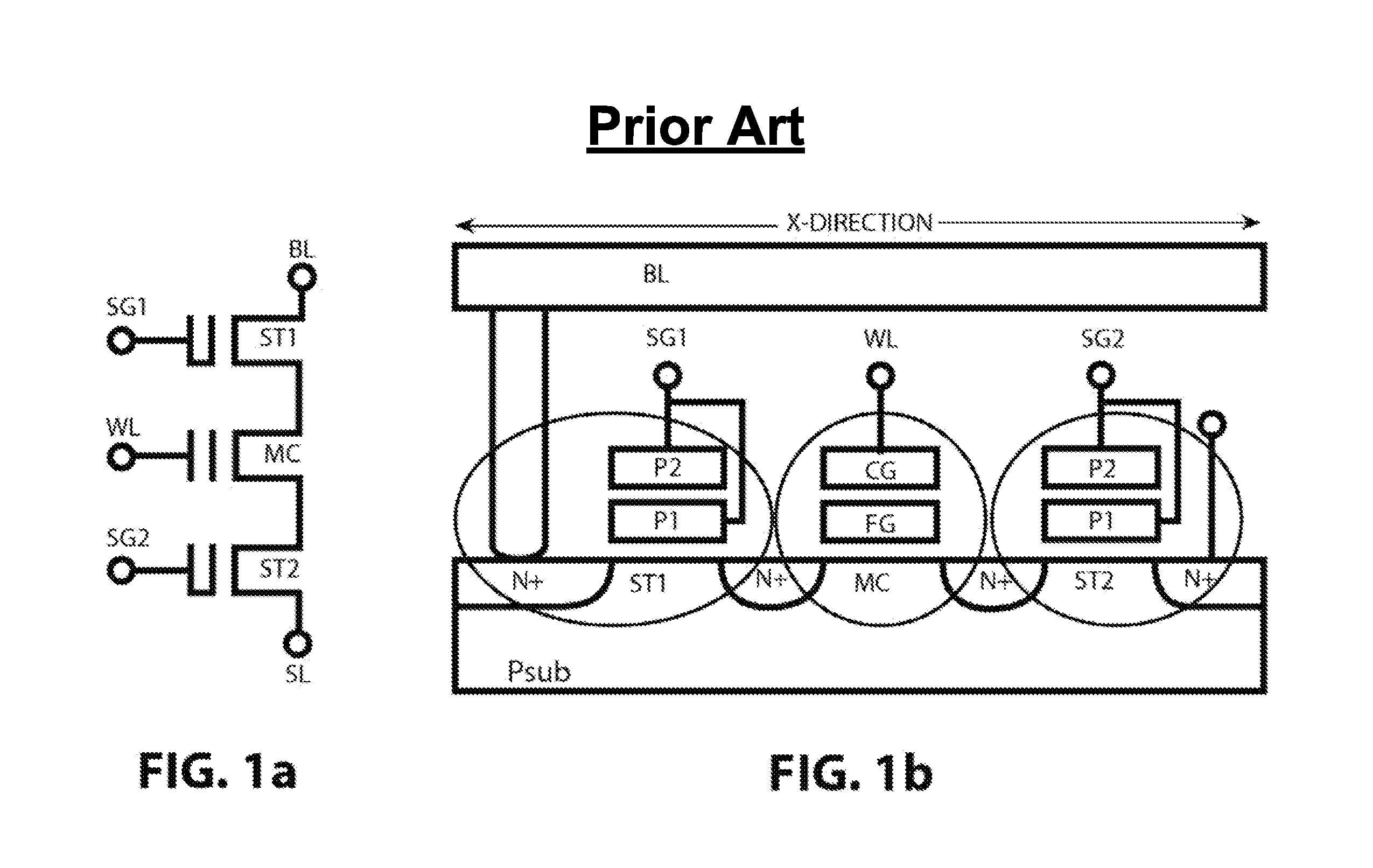
Although the traditional 2T Flotox-based EEPROM cell using the same low-current FN scheme for both Program and Erase operations, the cell size is too big.
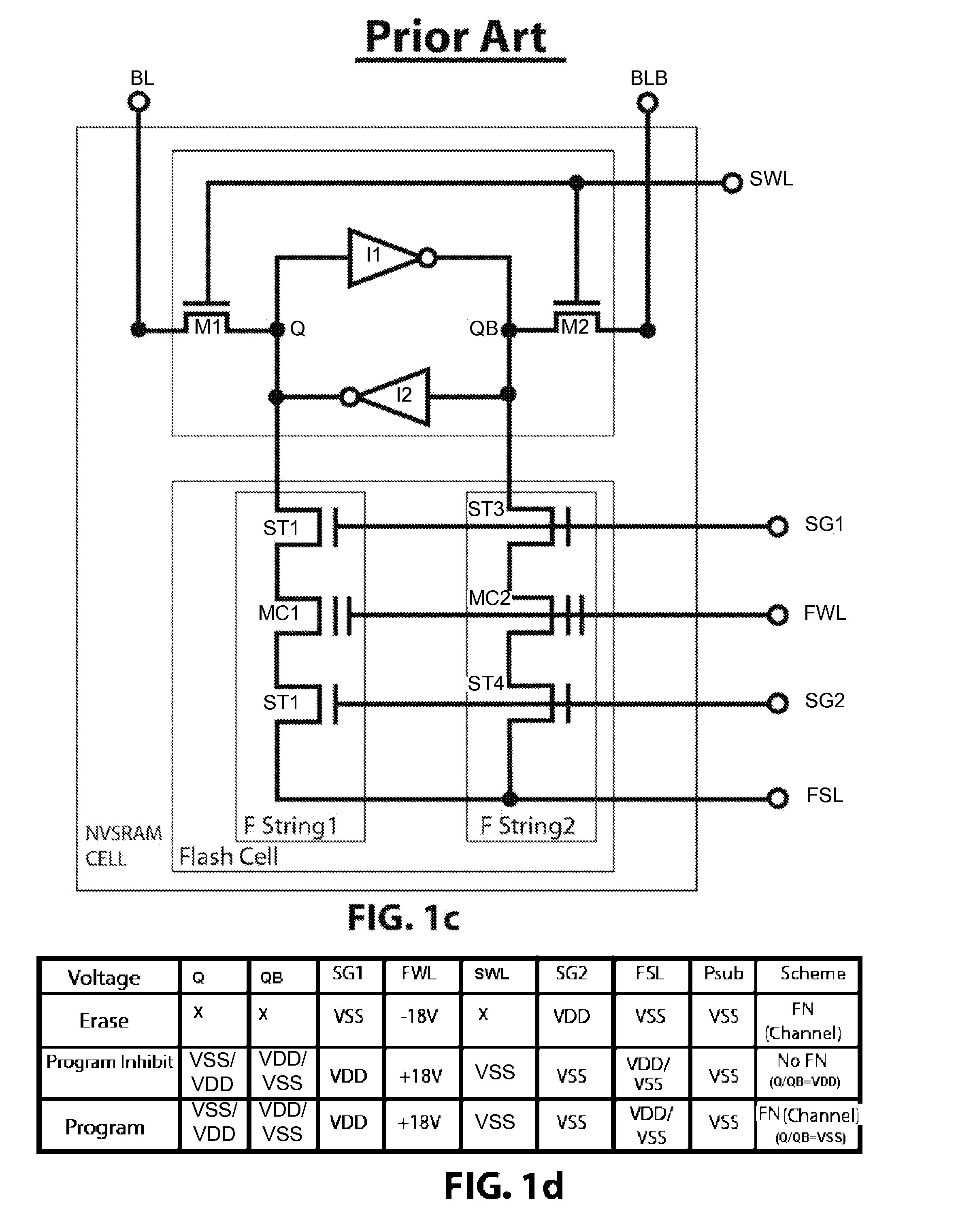
But for successfully operating down to 1.2V Vdd, the WL's Program voltage of 20V in NAND design is too high to reach during the power-down short period.

Method used


Image

  • Low-voltage fast-write nvsram cell
  • Low-voltage fast-write nvsram cell
  • Low-voltage fast-write nvsram cell

Examples


Embodiment Construction

[0053]The present invention is generally related with a novel design of static random-access memory (SRAM)-based non-volatile random-access memory (NVRAM) cell structure and array for an extremely fast write (program and erase) speed but low write and read voltage, for an extremely high-density, in-circuit or in-system programmable and erasable field-programmable gate array (FPGA) and NVRAM designs. More particularly, embodiments of the present invention provide a NVSRAM cell structure that is tailored for those SRAM-based FPGA IC designs with a stringent requirement of extremely high memory density of up to 1 Gb, a read operation with low-power Vdd down to 1.2V but with an extremely fast in-system repeatedly configurable speed of 10 ms.

[0054]More specifically, this invention is to provide a novel new SRAM-based NVRAM cell structure which is preferably comprised of one regular 6T SRAM CMOS cell and one pair of 4T Flash cell. Although the total number of transistors (T) of the presen...


PUM


Abstract

This invention discloses several embodiments of a low-voltage fast-write NVSRAM cells, made of either of a 2-poly floating-gate type flash cell or a 1-poly charge-trapping SONOS or MONOS flash cell with improvement by adding a Bridge circuit. This Bridge circuit is preferably inserted between each LV 6T SRAM cell and each HV Flash cell that comprises one paired complementary Flash strings. The Flash strings can be made of either 2T or 3T Flash strings. The tradeoff of using either a 2T or a 3T Flash string is subject to the gate area penalty and required design specs. One improvement for adding the Bridge circuit into the NVSRAM cell is to ensure the data writing between Flash cell and SRAM cell with the same polarity and to allow the operation down to low 1.2V Vdd.

Description

CROSS-REFERENCES TO RELATED APPLICATIONS[0001]This application claims priority to U.S. Provisional Patent Application No. 61 / 688,107, filed on May 7, 2012, commonly assigned, and hereby incorporated by reference in its entirety herein for all purposes.[0002]This application is related to U.S. Pat. Nos. 8,018,768, 7,760,540, 7,110,293, and 7,859,899.BACKGROUND OF THE INVENTION[0003]The present invention is generally related with a novel design of static random-access memory (SRAM)-based non-volatile random-access memory (NVRAM) cell structure and array for an extremely fast write (program and erase) speed but low write and read voltage, for an extremely high-density, in-circuit or in-system programmable and erasable field-programmable gate array (FPGA) and NVRAM designs.[0004]The LV SRAM-based FPGA is well known in the art. It is leading in the FPGA market place over today's HV Flash-based FPGA design. The LV SRAM-based FPGA cell and design achieves the highest cell's scalability dow...

Claims


Application Information

Patent Timeline
Patent Type & Authority Applications(United States)
IPC IPC(8): G11C16/04
CPCG11C16/0433G11C16/0466G11C11/005G11C14/0063
Inventor LEE, PETER WUNGTSAO, HSING-YA
Owner APLUS FLASH TECH
Learn More