
Lookup table and programmable logic device including lookup table

a programmable logic and lookup table technology, applied in the field of lookup table and programmable logic device including lookup table, can solve the problems that the arrangement of configuration data stored in the configuration memory has not been particularly considered so far, and achieve the optimization of the arrangement of configuration data stored in the configuration memory, reducing the number of “1” and reducing the power consumption of transfer.

Inactive Publication Date: 2013-11-07
SEMICON ENERGY LAB CO LTD
View PDF4 Cites 16 Cited by
  • Summary
  • Abstract
  • Description
  • Claims
  • Application Information

AI Technical Summary

Benefits of technology

The present invention relates to a method for reducing power consumption in a programmable logic device (PLD) by optimizing the arrangement of the configuration data stored in the device's configuration memory. Specifically, the method reduces the number of "1" values in the configuration data and avoids repetition of "0" values. This reduces power consumption during data transfer and programming of the PLD.

Problems solved by technology

However, the arrangement of the configuration data stored in the configuration memory has not been particularly considered so far.

Method used


Image

  • Lookup table and programmable logic device including lookup table
  • Lookup table and programmable logic device including lookup table
  • Lookup table and programmable logic device including lookup table

Examples


embodiment 1

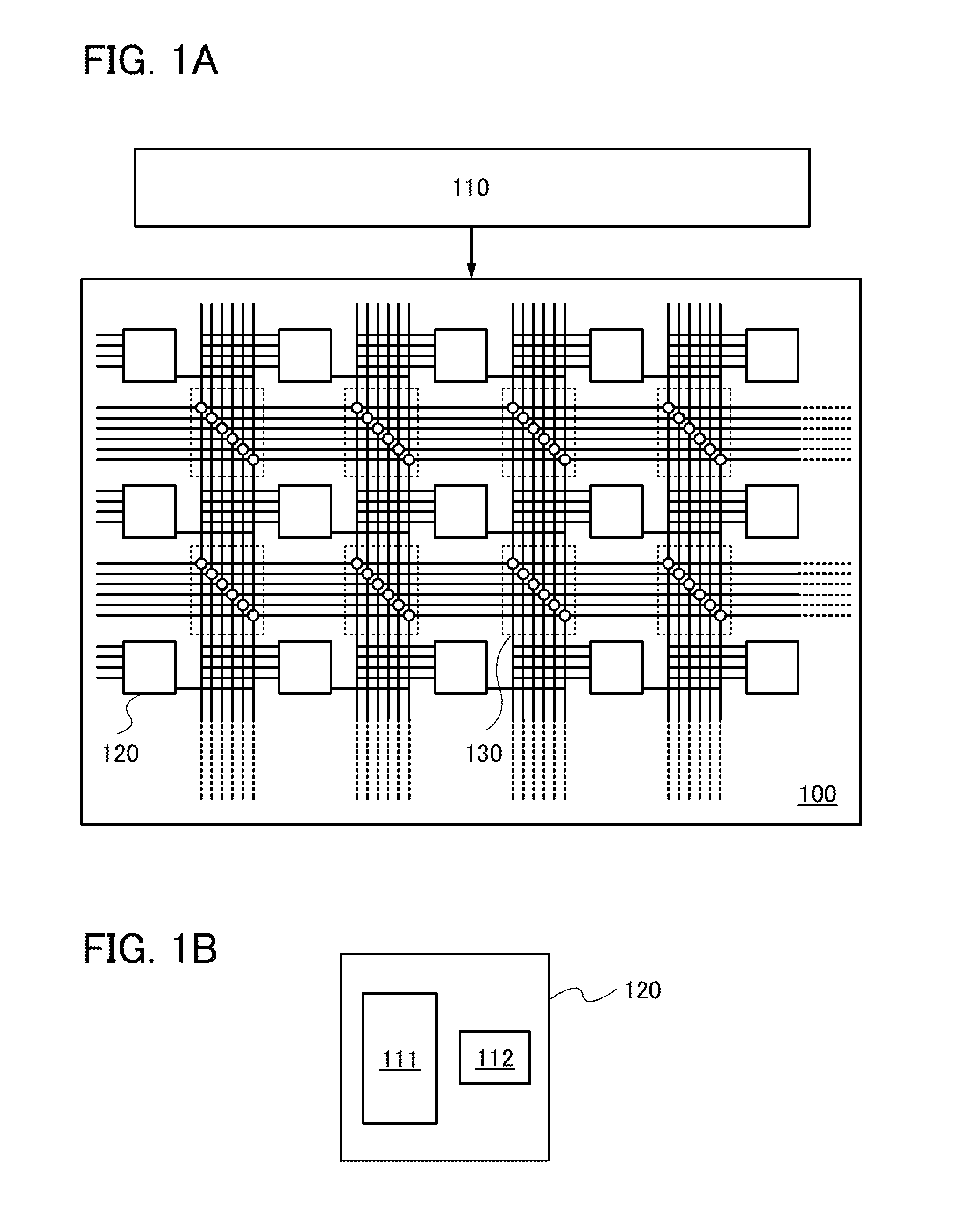
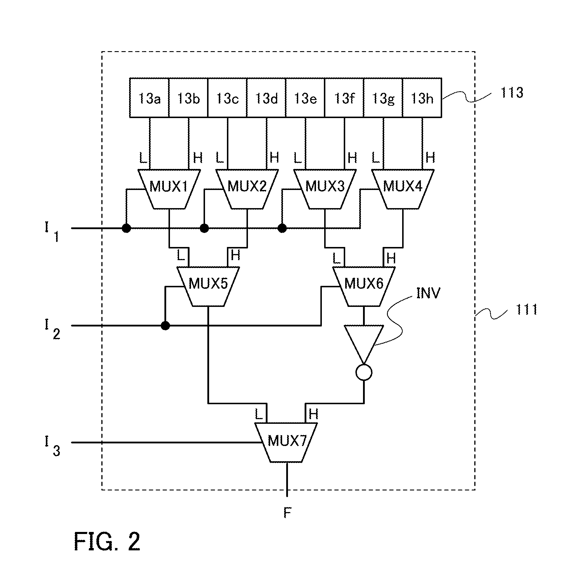
[0046]In this embodiment, a programmable logic device (PLD) of one embodiment of the present invention will be described with reference to FIGS. 1A and 1B, FIG. 2, FIG. 3, FIG. 4, FIG. 5, and FIG. 6.

[0047]FIG. 1A is a block diagram of one mode of a programmable logic device 100. The programmable logic device 100 includes a plurality of logic blocks 120 and a plurality of switch blocks 130. The plurality of logic blocks 120 are arranged in a matrix. A plurality of wirings are connected to the logic blocks 120, and the switch blocks 130 are provided at intersections of the wirings.

[0048]Further, the programmable logic device 100 may include a multiplier, a RAM block, a PLL block, or an I / O element. The multiplier has a function of multiplying a plurality of pieces of data at high speed. The RAM block has a function of storing given data as a memory. The PLL block has a function of supplying a clock signal to a circuit in the programmable logic device 100. The I / O element has a functio...

embodiment 2

[0100]In this embodiment, an example of a cross-sectional structure of a semiconductor device is described with reference to FIG. 7.

[0101]The semiconductor device illustrated in FIG. 7 is the memory element described in the above embodiment, in which the transistors are provided so as to overlap with one another. A lower part of the semiconductor device includes transistors including a first semiconductor material (e.g., silicon), and an upper part of the semiconductor device includes a transistor including a second semiconductor material (e.g., oxide semiconductor).

[0102]An n-channel transistor 510 includes a channel formation region 501 provided in a substrate 500 including a semiconductor material, low-concentration impurity regions 502 and high-concentration impurity regions 503 (collectively simply referred to as impurity regions in some cases) with the channel formation region 501 provided between the impurity regions, intermetallic compound regions 507 provided in contact wit...


PUM


Abstract

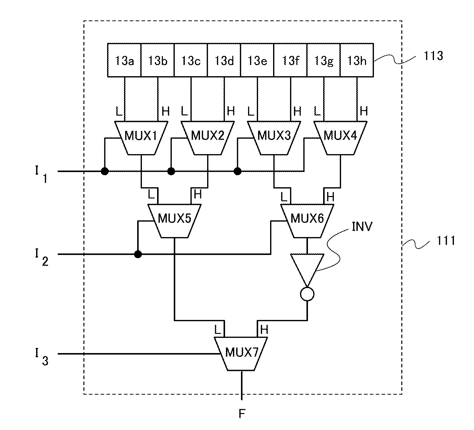
To optimize the arrangement of configuration data stored in a configuration memory. A lookup table includes a memory configured to store configuration data, a plurality of multiplexers each configured to select one signal from a plurality of input signals in accordance with the configuration data supplied from the memory and output the one signal, and an inverter. The plurality of multiplexers are connected in a binary tree with multiple levels. The inverter is provided between one of input terminals of a multiplexer in an uppermost level and an output terminal of a multiplexer in one level lower than the uppermost level. Signal selection is performed in each of the multiplexers so that the multiplexer in the uppermost level outputs, as an output signal, one signal of all input signals of the multiplexers in a lowermost level.

Description

BACKGROUND OF THE INVENTION[0001]1. Field of the Invention[0002]The present invention relates to a programmable logic device. Further, the present invention relates to a semiconductor device using the programmable logic device, and an electronic device using the semiconductor device.[0003]In this specification and the like, a semiconductor device means all types of devices that can function by utilizing semiconductor characteristics, and a transistor, a semiconductor circuit, and the like are each one form of the semiconductor device.[0004]2. Description of the Related Art[0005]Recently, a programmable logic device (PLD) such as a field programmable gate array (FPGA) or a complex programmable logic device (CPLD), in which the logic can be defined and changed by a user after manufacturing, has attracted attention to replace an application specific integrated circuit (ASIC) which is an integrated circuit for a specific use. The PLD has advantages such as reduction in development perio...

Claims


Application Information

Patent Timeline
IPC IPC(8): G11C7/10H03K19/08G11C11/24
CPCG11C7/10G11C11/24H03K19/08H03K19/1737H03K19/17728H03K19/1776H03K19/173
Inventor TAKEMURA, YASUHIKO
Owner SEMICON ENERGY LAB CO LTD
Learn More