Pipe register circuit and semiconductor memory apparatus having the same

Active Publication Date: 2013-10-24
SK HYNIX INC
View PDF3 Cites 1 Cited by
  • Summary
  • Abstract
  • Description
  • Claims
  • Application Information

AI Technical Summary

Benefits of technology

The patent describes two different types of circuits: a pipe register circuit and a semiconductor memory apparatus. These circuits are designed to improve the speed and reduce the area of a data output system. The first circuit helps to speed up the output of read data, while the second circuit helps to reduce the number of pads needed for data input and output. These circuits can be used in semiconductor memory devices to improve their performance and reduce their size.

Problems solved by technology

Furthermore, in the general semiconductor memory apparatus configured as above, there is delay, notably delay A and delay B, from when the read command is input to when the read data is output to an external, resulting in a reduction of the operation speed of the semiconductor memory apparatus.

Method used


Image

  • Pipe register circuit and semiconductor memory apparatus having the same
  • Pipe register circuit and semiconductor memory apparatus having the same
  • Pipe register circuit and semiconductor memory apparatus having the same

Examples


Embodiment Construction

[0024]Hereinafter, a pipe register circuit and a semiconductor memory apparatus according to the present invention will be described in detail with reference to the accompanying drawings through an exemplary embodiment.

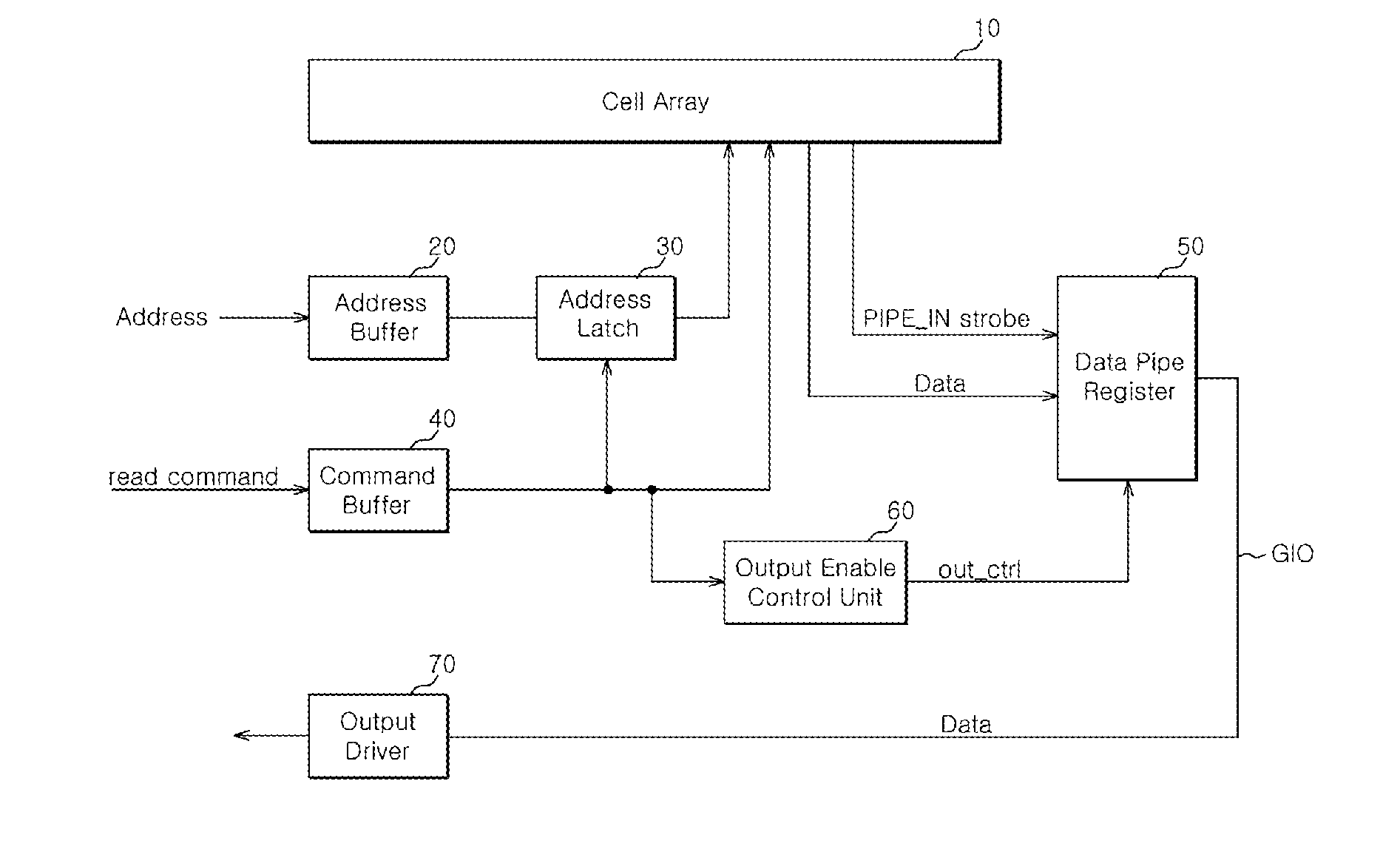
[0025]FIG. 3 is a block diagram illustrating a partial configuration of a semiconductor memory apparatus according to an embodiment.

[0026]Referring to FIG. 3, a semiconductor memory apparatus 300 according to the embodiment may include a cell array 310, an address buffer unit 320, an address latch unit 330, a command buffer unit 340, a pipe register 350, and an output driver 360.

[0027]The cell array 310 includes a plurality of memory cells arranged in order to store data.

[0028]The address buffer unit 320 is configured to receive an address signal address from an external, buffer the address signal, and output the buffered signal to the address latch unit 330.

[0029]The address latch unit 330 is configured to receive and latch the address signal address output from the ...


PUM


Abstract

A pipe register circuit includes an address storage section configured to temporarily and sequentially store address signals input from an external in correspondence with a read command signal input together with the address signals, and an address output control section configured to generate an address output control signal for allowing the address signals stored in the address storage section to be output in correspondence with CAS latency, and output the address output control signal to the address storage section.

Description

CROSS-REFERENCES TO RELATED APPLICATION[0001]The present application claims priority under 35 U.S.C. §119(a) to Korean application number 10-2012-0042119, filed on Apr. 23, 2012, in the Korean Intellectual Property Office, which is incorporated herein by reference in its entirety as set forth in full.BACKGROUND[0002]1. Technical Field[0003]The present invention relates to a semiconductor memory apparatus, and more particularly, to a pipe register circuit capable of improving an operation speed and a semiconductor memory apparatus having the same.[0004]2. Related Art[0005]In general, in a semiconductor memory apparatus such as a dynamic random access memory (DRAM), data stored in a cell is read through a data output circuit. When the stored data is read, the data is output after being delayed by a predetermined number of clocks from a clock, on which a read command is input, by CAS latency CL according to JEDEC specifications.[0006]FIG. 1 is a block diagram illustrating a part of a g...

Claims


Application Information

Patent Timeline
IPC IPC(8): G11C8/00G11C7/00
CPCG11C7/1039G11C7/106G11C7/20G11C7/222G11C11/4072G11C11/4076G11C11/4093G11C2207/2272G11C8/04G11C8/18G11C8/06
Inventor YOON, HYUN SU
Owner SK HYNIX INC
Why Eureka
Try Eureka