Semiconductor memory device for low voltage

Inactive Publication Date: 2006-10-05
SK HYNIX INC
View PDF19 Cites 6 Cited by
  • Summary
  • Abstract
  • Description
  • Claims
  • Application Information

AI Technical Summary

Benefits of technology

[0065] It is, therefore, an object of the present invention to provide a semiconductor memory device for improving an operational speed not using a high voltage under a low power supply voltage condition and for improving an operational margin at a read / write operation under the low power supply voltage condition.

Problems solved by technology

However, on the nano-technology based on under 100 nm, it is very difficult to develop the nano-technology.
That is, there is a limitation for integrating the semiconductor memory device more and more.
Also, a requested voltage level of the supply voltage becomes lower, e.g., from about 2.0 V to about 1.5 V or so far as about 1.0 V. Thus, the request about the supply voltage cannot be achieved by only developing the nano-technology.
If a voltage level of the supply voltage inputted to the semiconductor memory device is lower than a predetermined voltage level, an operating margin of each transistor included in the semiconductor memory device is not sufficient; and, as a result, a requested operation speed is not satisfied and an operation reliability of the semiconductor memory device is not guaranteed.
That is, as the voltage level of the supply voltage becomes lower, a little noise can seriously affect the operation reliability of the semiconductor memory device.
Therefore, there is a limitation for decreasing a voltage level of the supply voltage under a predetermined level.
If the bit line 17 and the gate electrode 13 in an unit cell are electronically short since an error is occurred under a manufacturing process, a current is flown continuously during the precharge step and a power consumption is increased.

Method used


Image

  • Semiconductor memory device for low voltage
  • Semiconductor memory device for low voltage
  • Semiconductor memory device for low voltage

Examples


Embodiment Construction

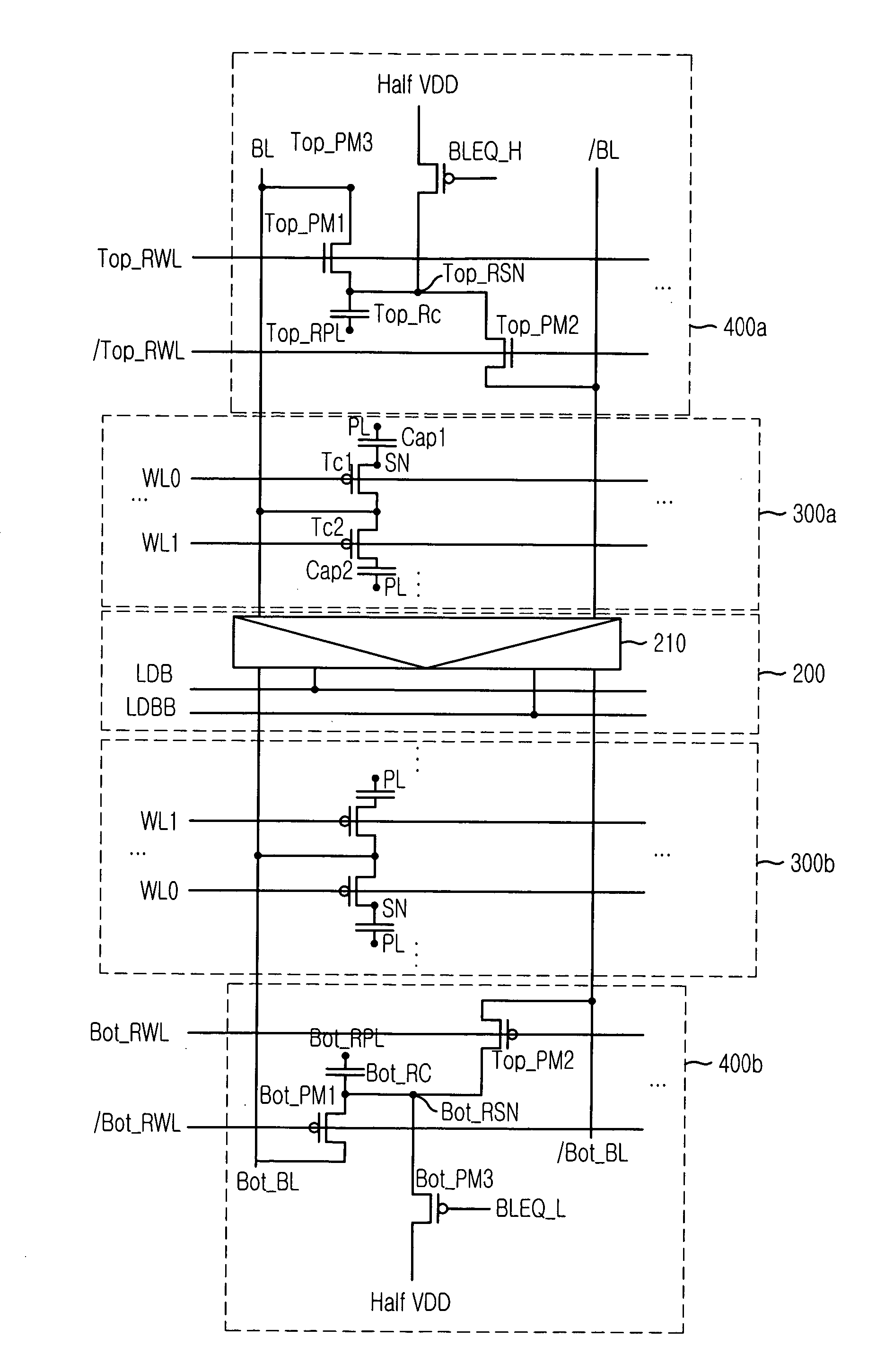
[0085] Hereinafter, a semiconductor memory device in accordance with the present invention will be described in detail referring to the accompanying drawings.

[0086]FIG. 7 is a block diagram showing a semiconductor memory device in accordance with an embodiment of the present invention.

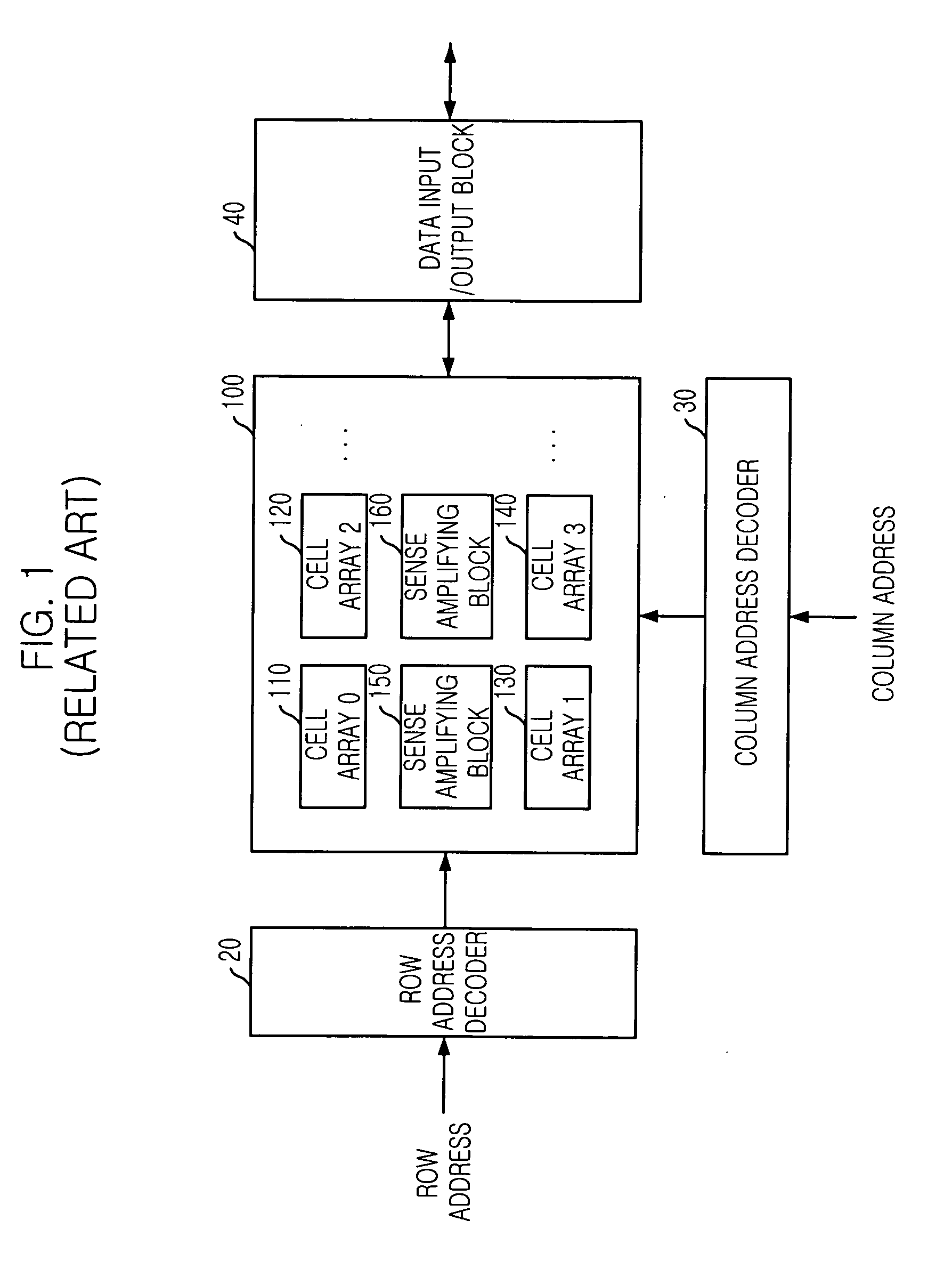
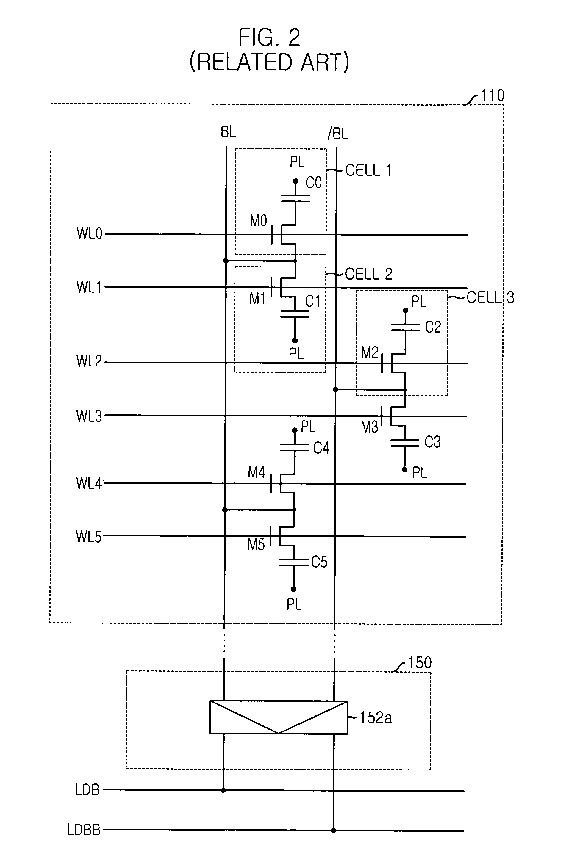
[0087] As shown, the semiconductor memory device includes a plurality of banks and each bank includes an X-decoder for receiving and decoding an X-address to thereby select a word line; an input / output (I / O) sense amplifying block for sensing and amplifying a data transferred by a selected bit line and for outputting the amplified data; and a Y-decoder for decoding a Y-address to thereby select a bit line.

[0088] Each bank further includes an input / output (I / O) switching unit for delivering a data transferred by a bit line to the I / O switching unit. The number of I / O switching units included in each bank corresponds to the number of first local data line pair SIO and SIOB.

[0089] Generally, the numbe...


PUM


Abstract

A semiconductor memory device includes a read amplifying unit for transferring a data from a local data line pair to a global data line as a read data; a write driver for transferring a write data from the global data line to the local data line pair; and an input / output (I / O) switching unit for transferring the read data from a segment data line pair to the local data line pair and for transferring the write data from the local data line pair to the segment data line pair, wherein each of the local data line pair and the segment line pair includes a VDD precharge block.

Description

FIELD OF THE INVENTION [0001] The present invention relates to a semiconductor memory device; and, more particularly, to a semiconductor memory device for efficiently operating under a low power supply voltage condition. DESCRIPTION OF RELATED ARTS [0002]FIG. 1 is a block diagram showing a core area of a conventional semiconductor memory device. [0003] As shown, the conventional semiconductor memory device includes a row address decoder 20, a column address decoder 30, a cell area 100 and a data input / output block 40. [0004] The cell area 100 includes a plurality of cell arrays, e.g., 110, 120, 130 and 140 and a plurality of sense amplifying blocks, e.g., 150 and 160. The row address decoder 20 receives a row address and decodes the row address in order to access a data stored in the cell area 100; and the column address decoder 30 receives a column address and decodes the column address in order to access the data stored in the cell area 100. The data input / output block 40 is for o...

Claims


Application Information

Patent Timeline
IPC IPC(8): G11C11/24
CPCG11C11/4096G11C2207/005G11C2207/002G11C11/4097G11C7/06G11C7/10G11C7/12
Inventor KANG, HEE-BOKAHN, JIN-HONG
Owner SK HYNIX INC
Why Eureka
Try Eureka