
Dynamic bank mode addressing for memory access

a dynamic bank and memory access technology, applied in the field of parallel processing, can solve problems such as reducing performance and conflicting banks

Active Publication Date: 2013-10-10
NVIDIA CORP
View PDF3 Cites 21 Cited by
  • Summary
  • Abstract
  • Description
  • Claims
  • Application Information

AI Technical Summary

Benefits of technology

The patent text describes a system and method for accessing a multi-bank memory in a way that allows different programs to avoid conflicts. The system uses a bank mode that defines the number of bits per bank, and the system dynamically maps the program's addresses to the banks based on this mode. This allows each program to access the memory independently without causing conflicts. The technical effect of this system is improved performance and reliability for parallel threads accessing a multi-bank memory.

Problems solved by technology

If multiple threads need to access two or more locations in the same bank of memory than can be accessed in a single clock cycle, a bank conflict exists.
When bank conflicts do occur, the accesses for addresses mapped to the same bank must be completed in separate clock cycles, thereby reducing performance.

Method used


Image

  • Dynamic bank mode addressing for memory access
  • Dynamic bank mode addressing for memory access
  • Dynamic bank mode addressing for memory access

Examples


Embodiment Construction

[0022]In the following description, numerous specific details are set forth to provide a more thorough understanding of the present invention. However, it will be apparent to one of skill in the art that the present invention may be practiced without one or more of these specific details.

System Overview

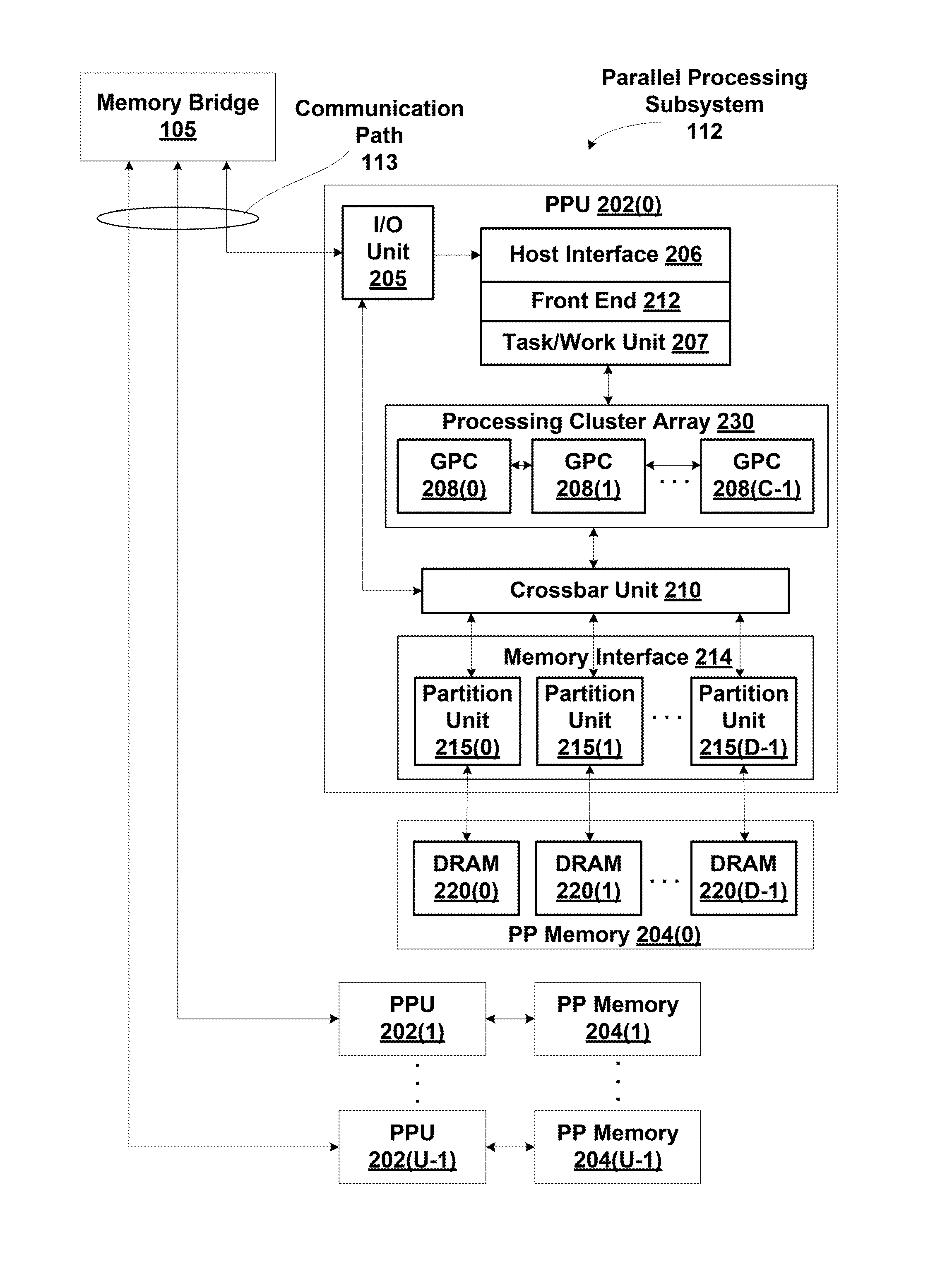
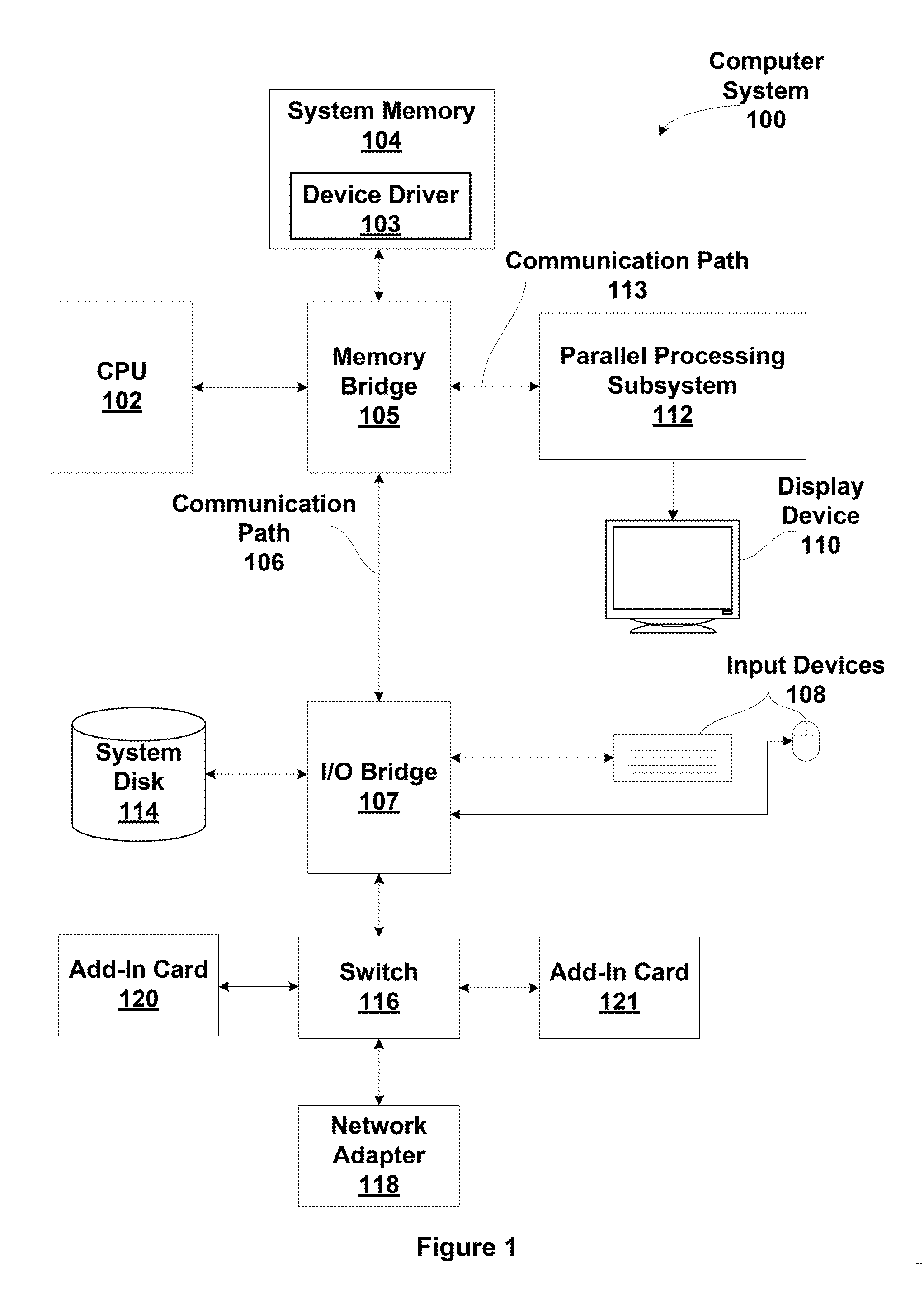
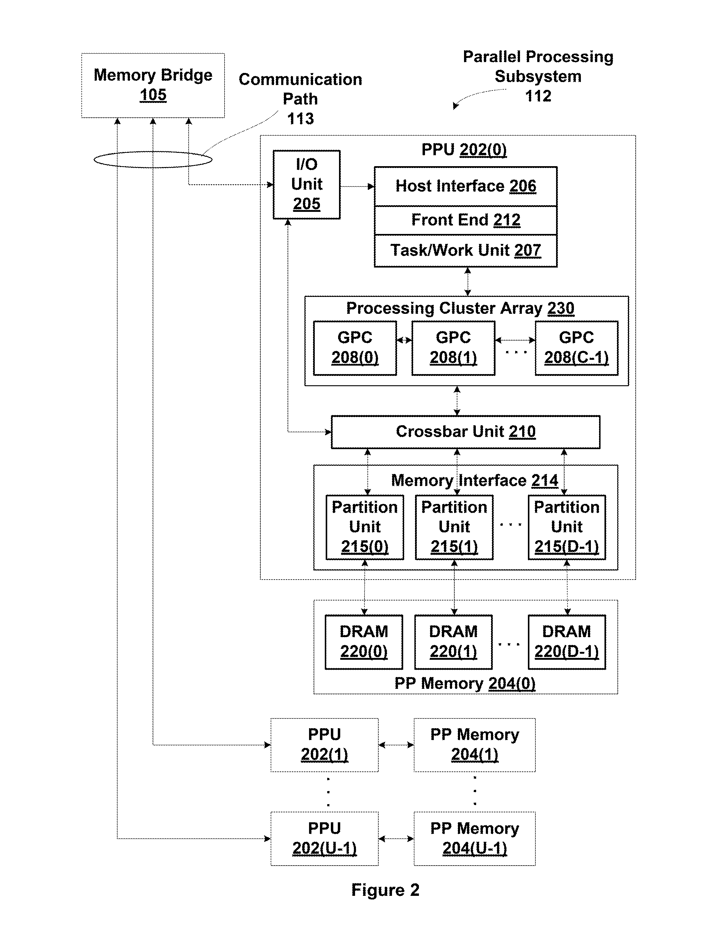
[0023]FIG. 1 is a block diagram illustrating a computer system 100 configured to implement one or more aspects of the present invention. Computer system 100 includes a central processing unit (CPU) 102 and a system memory 104 communicating via an interconnection path that may include a memory bridge 105. Memory bridge 105, which may be, e.g., a Northbridge chip, is connected via a bus or other communication path 106 (e.g., a HyperTransport link) to an I / O (input / output) bridge 107. I / O bridge 107, which may be, e.g., a Southbridge chip, receives user input from one or more user input devices 108 (e.g., keyboard, mouse) and forwards the input to CPU 102 via communication path 106 and m...


PUM


Abstract

One embodiment sets forth a technique for dynamically mapping addresses to banks of a multi-bank memory based on a bank mode. Application programs may be configured to perform read and write a memory accessing different numbers of bits per bank, e.g., 32-bits per bank, 64-bits per bank, or 128-bits per bank. On each clock cycle an access request may be received from one of the application programs and per processing thread addresses of the access request are dynamically mapped based on the bank mode to produce a set of bank addresses. The bank addresses are then used to access the multi-bank memory. Allowing different bank mappings enables each application program to avoid bank conflicts when the memory is accesses compared with using a single bank mapping for all accesses.

Description

BACKGROUND OF THE INVENTION[0001]1. Field of the Invention[0002]The present invention generally relates to parallel processing and, more specifically, to a parallel architecture that supports dynamic bank address mapping for multi-bank memory accesses.[0003]2. Description of the Related Art[0004]In a single-instruction multiple-thread (SIMT) processing environment, threads are organized in groups of P parallel threads called warps that execute the same program. Although the P threads of a thread group execute each instruction of the program in parallel, each thread of a thread group independently executes the instruction using its own data and registers. Each thread in the thread group is configured to access a multi-bank memory using a fixed mapping of per-thread addresses to the banks of the multi-bank memory. If multiple threads need to access two or more locations in the same bank of memory than can be accessed in a single clock cycle, a bank conflict exists.[0005]Application pr...

Claims


Application Information

Patent Timeline
IPC IPC(8): G06F12/06
CPCG06F9/38G06F9/3887G06F9/3851
Inventor FETTERMAN, MICHAELCARLTON, STEWART GLENNHAHN, DOUGLAS J.SELVANESAN, RAJESHWARANGADRE, SHIRISHHEINRICH, STEVEN JAMES
Owner NVIDIA CORP
Learn More