Electro-optical device, shift register circuit, and semiconductor device
a technology of shift register and transistor, applied in static indicating devices, instruments, time-delay networks, etc., can solve the problem that the control electrode of the transistor b>204/b> is not sufficiently charged when the shift register is switched, and achieve the effect of preventing the rising speed of the gate line selection signal from decreasing
- Summary
- Abstract
- Description
- Claims
- Application Information
AI Technical Summary
Benefits of technology
Problems solved by technology
Method used
Image
Examples
first embodiment
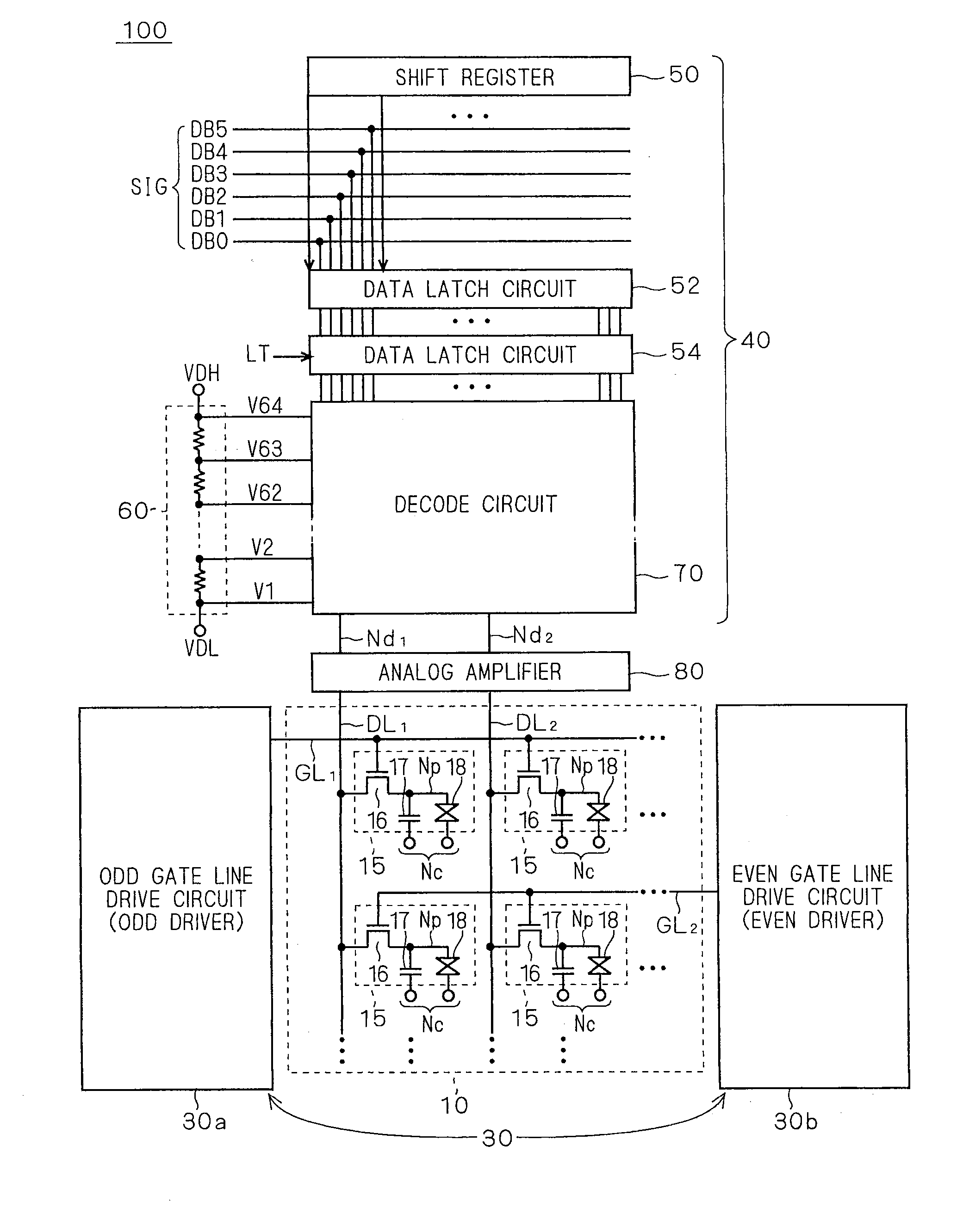
[0062]FIG. 1 is a schematic block diagram showing a configuration of a display device according to the present invention, and shows an entire configuration of a liquid crystal display device as a representative example of the display device. In addition, the present invention is not limited to the liquid crystal display device, and it may be widely applied to display devices to convert an electric signal to brightness of light, such as an electroluminescence (EL), organic EL, plasma display, and electronic paper, or electro-optical devices to convert intensity of light to an electric signal, such as an image capturing apparatus (imaging sensor).
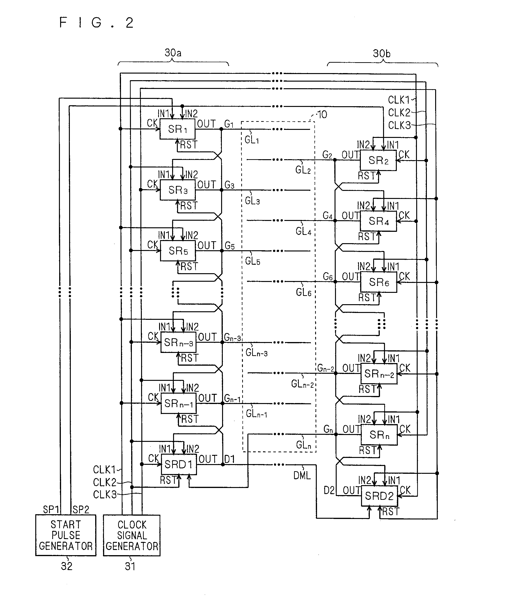
[0063]A liquid crystal display device 100 includes a liquid crystal array section 10, a gate line drive circuit 30, and a source driver 40. The liquid crystal array section 10 includes a plurality of pixels 15 arranged in the form a matrix. Gate lines GL1, GL2 . . . (referred to as the “gate line GL” collectively) are provided for rows of the...
second embodiment
[0169]According to a second embodiment, a shift register capable of changing a shift direction of a signal is applied to the present invention. A gate line drive circuit 30 using such shift register is capable of bidirectional scanning. A direction from head to bottom (order of gate lines GL1, GL2, GL3 . . . ) is defined as a “forward direction”, and a direction from bottom to head (order of gate lines GLn, GLn−1, GLn−2 . . . ) is defined as a “backward direction”.
[0170]FIG. 12 is a drawing showing a configuration of the gate line drive circuit 30 according to the second embodiment. This gate line drive circuit 30 is also composed of an odd driver 30a having cascaded unit shift registers SR1, SR3, SR5 . . . to drive the gate lines GL1, GL3, GL5 . . . in the odd rows, and an even driver 30b having cascaded unit shift registers SR2, SR4, SR6 . . . to drive the gate lines GL2, GL4, GL6 . . . in the even rows.
[0171]In addition, control signals (first and second voltage signals Vn and Vr...
third embodiment
[0214]According to a third embodiment, the present invention is applied to a gate line drive circuit composed of unit shift registers SR capable of bidirectional scanning without using a switching circuit. Since a signal delay due to the switching circuit is not generated in each unit shift register, the same response speed as that of a usual unit shift register (performing only one directional shift) can be obtained. Such unit shift register is disclosed in Japanese Patent Application Laid-Open No. 2008-287753 according to the idea of the inventor of the present invention.
[0215]FIG. 14 is a circuit diagram of a unit shift register SRk according to the third embodiment, in which the present invention is applied to the circuit in FIG. 3 of Japanese Patent Application Laid-Open No. 2008-287753. The unit shift register SRk is also composed of an output circuit 20, a pull-up drive circuit 21, and a pull-down drive circuit 22, and the pull-up drive circuit 21 includes a forward pull-up d...
PUM
 Abstract
Description
Claims
Application Information
 - R&D
- Intellectual Property
- Life Sciences
- Materials
- Tech Scout
- Unparalleled Data Quality
- Higher Quality Content
- 60% Fewer Hallucinations
Browse by: Latest US Patents, China's latest patents, Technical Efficacy Thesaurus, Application Domain, Technology Topic, Popular Technical Reports.
© 2025 PatSnap. All rights reserved.Legal|Privacy policy|Modern Slavery Act Transparency Statement|Sitemap|About US| Contact US: help@patsnap.com


