
Flowable silicon-and-carbon-containing layers for semiconductor processing

a technology of silicon and carbon-containing layers, which is applied in the direction of semiconductor/solid-state device manufacturing, basic electric elements, electric apparatus, etc., can solve the problems of increasing the difficulty of filling the gap with dielectric materials and the width of the structure of the device, and achieves the effect of reducing the beneficially low wet etch rate and reducing the hydrogen conten

Inactive Publication Date: 2013-08-22
APPLIED MATERIALS INC
View PDF4 Cites 378 Cited by
  • Summary
  • Abstract
  • Description
  • Claims
  • Application Information

AI Technical Summary

Benefits of technology

The patent describes a method for creating a layer of silicon and carbon on a semiconductor substrate using a precursor that is activated by a remote plasma. This method leads to the formation of a flowable layer that can fill high-aspect ratio gaps on the substrate with fewer voids and weak seams. The hydrogen content in the layer can then be reduced through curing treatments. The absence of oxygen in the layer also results in a lower wet etch rate compared to silicon oxide and silicon.

Problems solved by technology

The decreasing feature sizes result in structural features on the device having decreased width.
The widths of gaps and trenches on the device narrow such that filling the gap with dielectric material becomes more challenging.
The depositing dielectric material is prone to clog at the top before the gap completely tills, producing a void or seam in the middle of the gap.

Method used


Image

  • Flowable silicon-and-carbon-containing layers for semiconductor processing
  • Flowable silicon-and-carbon-containing layers for semiconductor processing
  • Flowable silicon-and-carbon-containing layers for semiconductor processing

Examples


Embodiment Construction

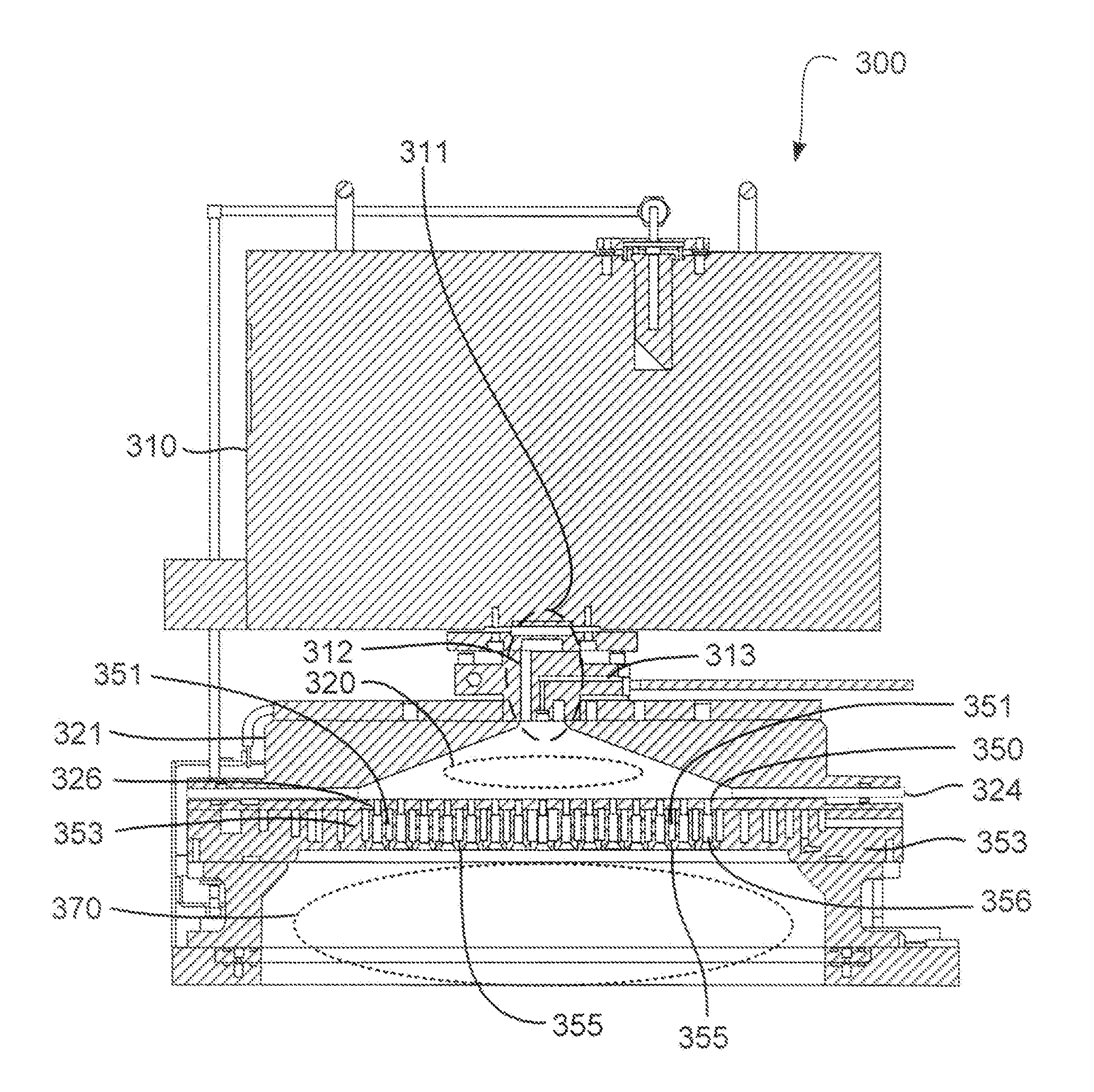
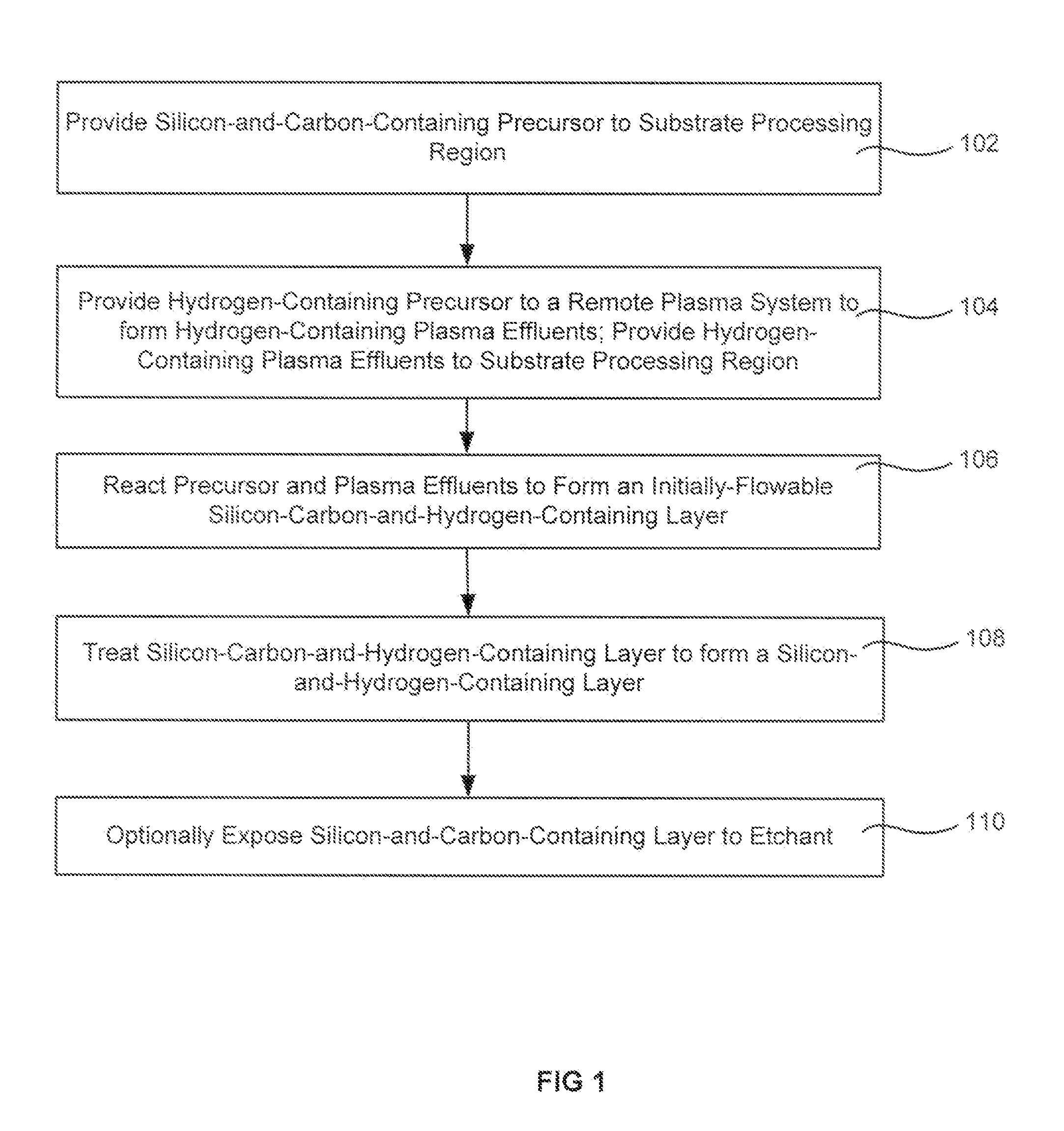
[0013]Methods are described for forming and curing a gapfill silicon-and-carbon-containing layer on a semiconductor substrate. The silicon and carbon constituents may come from a silicon-and-carbon-containing precursor excited by a radical hydrogen precursor that has been activated in a remote plasma region. Exemplary precursors include 1,3,5-trisilapentane (H3Si—CH2—SiH2—CH2—SiH3) as the silicon-and-carbon-containing precursor and hydrogen (H2) as the hydrogen-containing precursor. The hydrogen-containing precursor may also be a hydrocarbon, such as acetylene (C2H2) or ethylene (C2H4). The hydrogen-containing precursor is passed through a remote plasma region to form plasma effluents (the radical hydrogen precursor) which are flowed into the substrate processing region. When the silicon-and-carbon-containing precursor combines with the plasma effluents in the substrate processing region, they form a flowable silicon-carbon-and-hydrogen-containing layer on the semiconductor substrat...


PUM


Abstract

Methods are described for forming and curing a gapfill silicon-and-carbon-containing layer on a semiconductor substrate. The silicon and carbon constituents may come from a silicon-and-carbon-containing precursor excited by a radical hydrogen precursor that has been activated in a remote plasma region. Exemplary precursors include 1,3,5-trisilapentane (H3Si—CH2—SiH2—CH2—SiH3) as the silicon-and-carbon-containing precursor and hydrogen (H2) as the hydrogen-containing precursor. The hydrogen-containing precursor may also be a hydrocarbon, such as acetylene (C2H2) or ethylene (C2H4). The hydrogen-containing precursor is passed through a remote plasma region to form plasma effluents (the radical hydrogen precursor) which are flowed into the substrate processing region. When the silicon-and-carbon-containing precursor combines with the plasma effluents in the substrate processing region, they form a flowable silicon-carbon-and-hydrogen-containing layer on the semiconductor substrate.

Description

CROSS-REFERENCES TO RELATED APPLICATIONS[0001]This application claims the benefit of U.S. Provisional Application No. 61 / 536,380, filed Sep. 19, 2011, and titled “FLOWABLE SILICON-AND-CARBON—CONTAINING LAYERS FOR SEMICONDUCTOR PROCESSING.” This application also claims the benefit of U.S. Provisional Application No. 61 / 532,708 by Mallick et al, filed Sep. 9, 2011 and titled “FLOWABLE SILICON-CARBON-NITROGEN LAYERS FOR SEMICONDUCTOR PROCESSING.” This application also claims the benefit of U.S. Provisional Application No. 61 / 550,755 by Underwood et al, tiled Oct. 24, 2011 and titled “TREATMENTS FOR DECREASING ETCH RATES AFTER FLOWABLE DEPOSITION OF SILICON-CARBON-AND-NITROGEN-CONTAINING LAYERS.” This application also claims the benefit of U.S. Provisional Application No. 61 / 567,738 by Underwood et al. filed Dec. 7, 2011 and titled “DOPING OF DIELECTRIC LAYERS.” Each of the above U.S. Provisional Applications is incorporated herein in its entirety for all purposes.BACKGROUND OF THE INVE...

Claims


Application Information

Patent Timeline
IPC IPC(8): H01L21/02
CPCH01L21/02123H01L21/02167H01L21/02211H01L21/02274H01L21/02348H01L21/76837H01L21/02271
Inventor MALLICK, ABHIJIT BASUINGLE, NITIN K.
Owner APPLIED MATERIALS INC
Learn More