Semiconductor Substrate, Integrated Circuit Having the Semiconductor Substrate, and Methods of Manufacturing the Same

Active Publication Date: 2013-08-08
INST OF MICROELECTRONICS CHINESE ACAD OF SCI
View PDF4 Cites 187 Cited by
  • Summary
  • Abstract
  • Description
  • Claims
  • Application Information

AI Technical Summary

Benefits of technology

This patent is about a new semiconductor substrate and method of manufacturing it that reduces the area occupied by transistors in an integrated circuit. By using this method, it is unnecessary to separately provide for each transistor a conductive contact for the back-gate in the manufacturing process. Instead, the back-gates of at least some transistors can be connected to a common interconnection layer, which can be connected to outside through one contact. This reduces the area occupied by the transistors and increases the utilization ratio of the wafer. The patent describes a method that can be used to manufacture a semiconductor substrate that is more efficient in terms of the area it occupies. This can lead to higher utilization of the semiconductor wafer, which is the starting material for integrated circuits.

Problems solved by technology

However, the reduction in the length of the gate electrode will result in a short-channel effect, thus degrading the performance of the semiconductor device and the whole integrated circuit.
However, according to conventional methods, in order to connect the ground planes of the NMOSFET and PMOSFET to the respective voltage sources, extra contacts and wirings are needed, resulting in an increase in the area occupied by the device.

Method used


Image

  • Semiconductor Substrate, Integrated Circuit Having the Semiconductor Substrate, and Methods of Manufacturing the Same
  • Semiconductor Substrate, Integrated Circuit Having the Semiconductor Substrate, and Methods of Manufacturing the Same
  • Semiconductor Substrate, Integrated Circuit Having the Semiconductor Substrate, and Methods of Manufacturing the Same

Examples


first embodiment

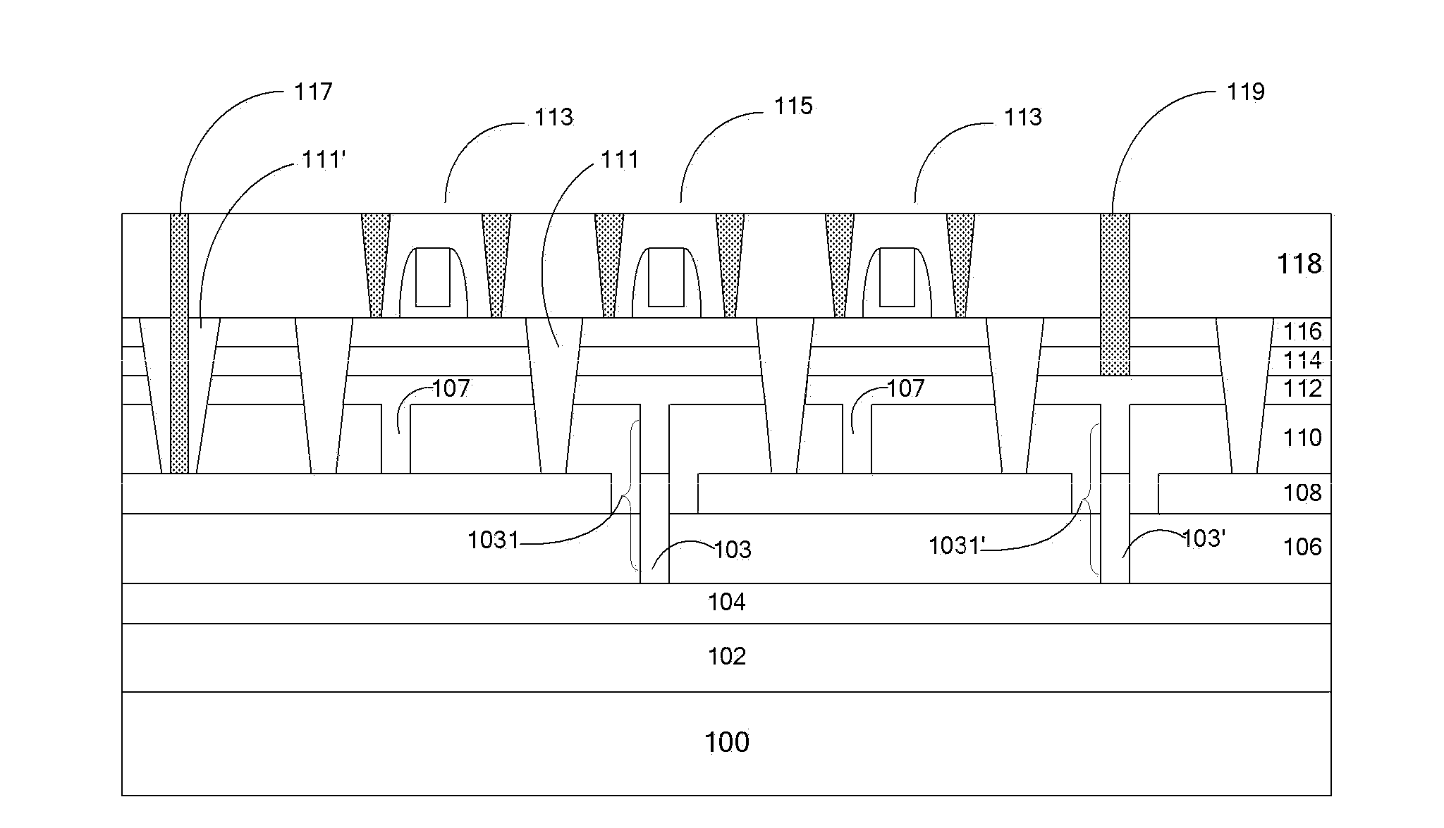
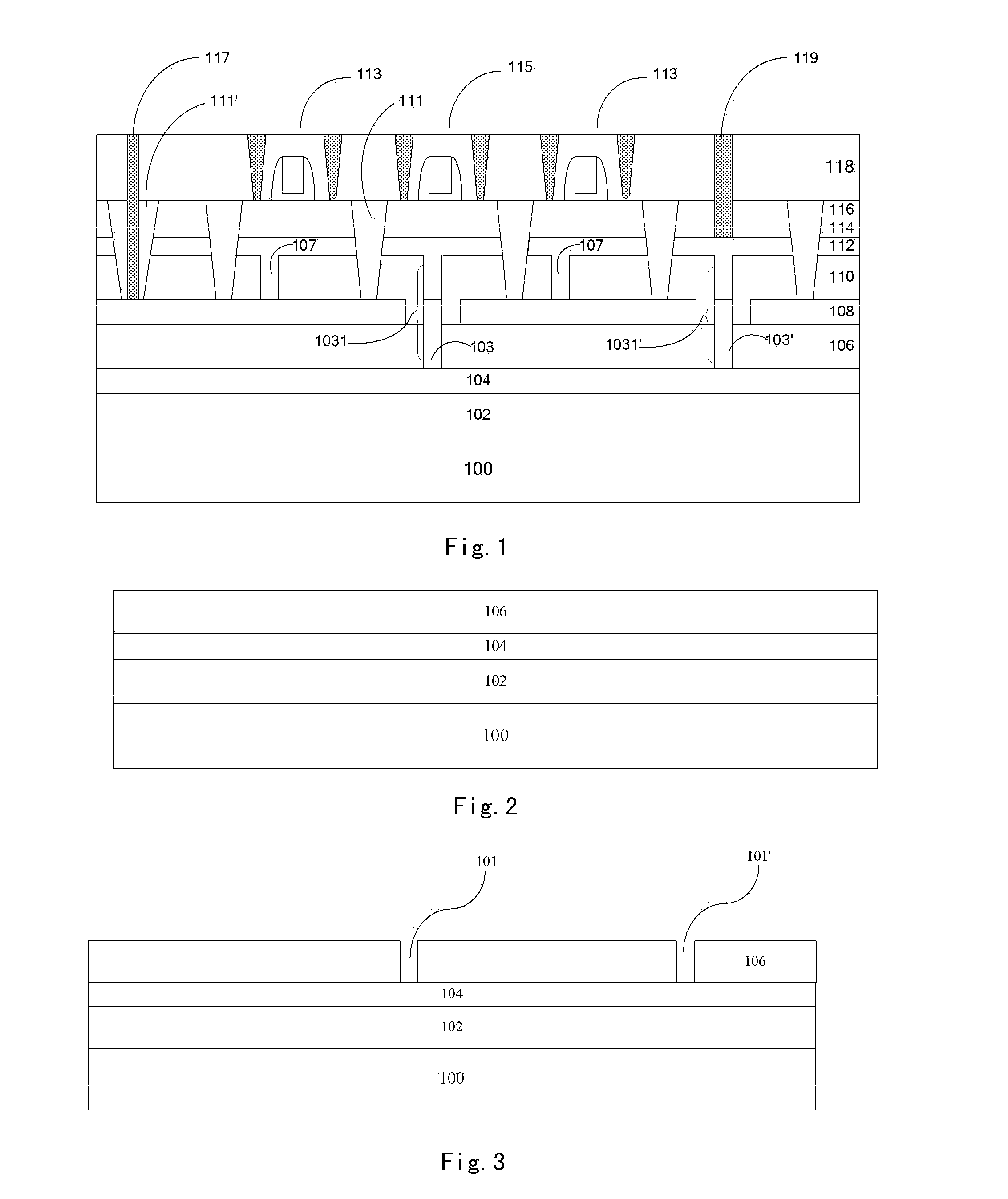
[0022]FIG. 1 shows a schematic cross-sectional view of an integrated circuit 10 comprising transistors having back-gates according to a first embodiment of the present invention.

[0023]The integrated circuit 10 comprises: a semiconductor base layer 100; a first insulating material layer 102 on the semiconductor base layer 100; a first conductive material layer 104 on the first insulating material layer 102; a second insulating material layer 106 on the first conductive material layer 104; a second conductive material layer 108 on the second insulating material layer 106; a third insulating material layer 110 on the second conductive material layer 108; a third conductive material layer 112 on the third insulating material layer 110; an insulating buried layer 114 on the third conductive material layer 112; a semiconductor layer 116 formed on the insulating buried layer 114.

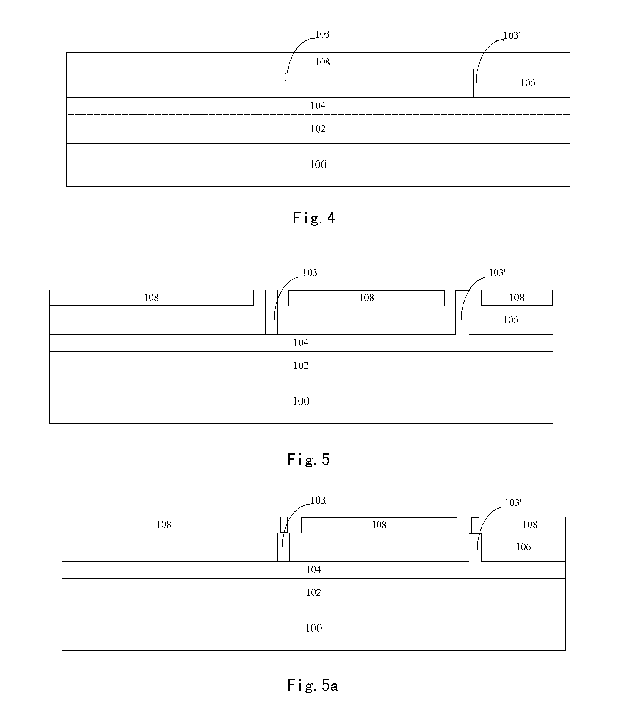
[0024]The integrated circuit 10 further comprises vias 107 penetrating through the third insulating material lay...

second embodiment

[0043]In the first embodiment described above, the back-gates of the transistors of the first and second conductive types are all connected to outside through the conductive material layer thereunder, but the present invention is not limited to this, it also allows the back-gates of only transistors of the first conductive type or the back-gates of only transistors of the second conductive type to be connected to outside through the conductive material layer thereunder.

[0044]FIG. 11 shows a schematic cross-sectional view of an integrated circuit 20 comprising transistors having back-gates according to a second embodiment of the present invention.

[0045]The integrated circuit 20 comprises: a semiconductor base layer 200; a first insulating material layer 202 on the semiconductor base layer 200; a first conductive material layer 204 on the first insulating material layer 202; a second insulating material layer 206 on the first conductive material layer 204; a second conductive material...


PUM


Abstract

The present invention relates to a semiconductor substrate, an integrated circuit having the semiconductor substrate, and methods of manufacturing the same. The semiconductor substrate for use in an integrated circuit comprising transistors having back-gates according to the present invention comprises: a semiconductor base layer; a first insulating material layer on the semiconductor base layer; a first conductive material layer on the first insulating material layer; a second insulating material layer on the first conductive material layer; a second conductive material layer on the second insulating material layer; an insulating buried layer on the second conductive material layer; and a semiconductor layer on the insulating buried layer, wherein at least one first conductive via is provided between the first conductive material layer and the second conductive material layer to penetrate through the second insulating material layer so as to connect the first conductive material layer with the second conductive material layer, the position of each of the first conductive vias being defined by a region in which a corresponding one of a first group of transistors is to be formed.

Description

FIELD OF THE INVENTION[0001]The present invention relates to the field of semiconductor fabrication, and more particularly, to a semiconductor substrate, an integrated circuit having the semiconductor substrate, and methods of manufacturing the same.BACKGROUND OF THE INVENTION[0002]Generally, an integrated circuit (IC) includes a combination of an NMOS (n type Metal-Oxide-Semiconductor) transistor and a PMOS (p type Metal-Oxide-Semiconductor) transistor formed on a substrate. In order to increase the efficiency of the very large scale integrated circuits and to reduce the manufacturing costs thereof, a continuous trend is to reduce the feature size of the device, especially the length of the gate electrode. However, the reduction in the length of the gate electrode will result in a short-channel effect, thus degrading the performance of the semiconductor device and the whole integrated circuit.[0003]The Silicon-On-Insulator (SOI) technique is to introduce a buried oxide layer (BOX) ...

Claims


Application Information

Patent Timeline
IPC IPC(8): H01L27/12H01L27/092H01L21/762
CPCH01L21/762H01L27/12H01L27/092H01L21/743H01L29/78648H01L2924/0002H01L21/84H01L27/1203H01L2924/00
Inventor ZHU, HUILONGLUO, ZHIJIONGYIN, HAIZHOUZHONG, HUICAI
Owner INST OF MICROELECTRONICS CHINESE ACAD OF SCI
Why Eureka
Try Eureka