Resist coating and developing apparatus, resist coating and developing method, resist-film processing apparatus, and resist-film processing method
a technology of resist coating and developing apparatus, applied in the direction of photomechanical apparatus, printing, instruments, etc., can solve the problems of deteriorating properties as an integrated circuit, affecting the properties of a semiconductor device to be manufactured, and the inability to transfer the desired shape to a base layer, etc., to reduce the roughness of the resist pattern on the line width
- Summary
- Abstract
- Description
- Claims
- Application Information
AI Technical Summary
Benefits of technology
Problems solved by technology
Method used
Image
Examples
experiment 1
[0078]In Experiment 1, a resist film on a wafer which had been subjected up to the supply of the solvent gas, and a resist film on a wafer which had been subjected up to the supply of the release liquid were compared to each other. FIG. 9 show the result. FIG. 9(a) shows a cross-section of the resist film (a line part of the resist pattern) after the supply of the solvent gas, and FIG. 9(b) shows a cross-section of the resist film (a line part of the resist pattern) after the supply of the release liquid. See, particularly the sectional shapes indicated by the arrows in the drawings. The resist cross-section shown in FIG. 9(a) has a bell-like shape because of the supply of the solvent gas. On the other hand, the resist cross-section shown in FIG. 9(b) after the supply of the release liquid has substantially a rectangular shape, although an upper part thereof is somewhat rounded. Namely, the following facts can be understood. Since the parts dissolved by the solvent gas sagged, the c...
experiment 2
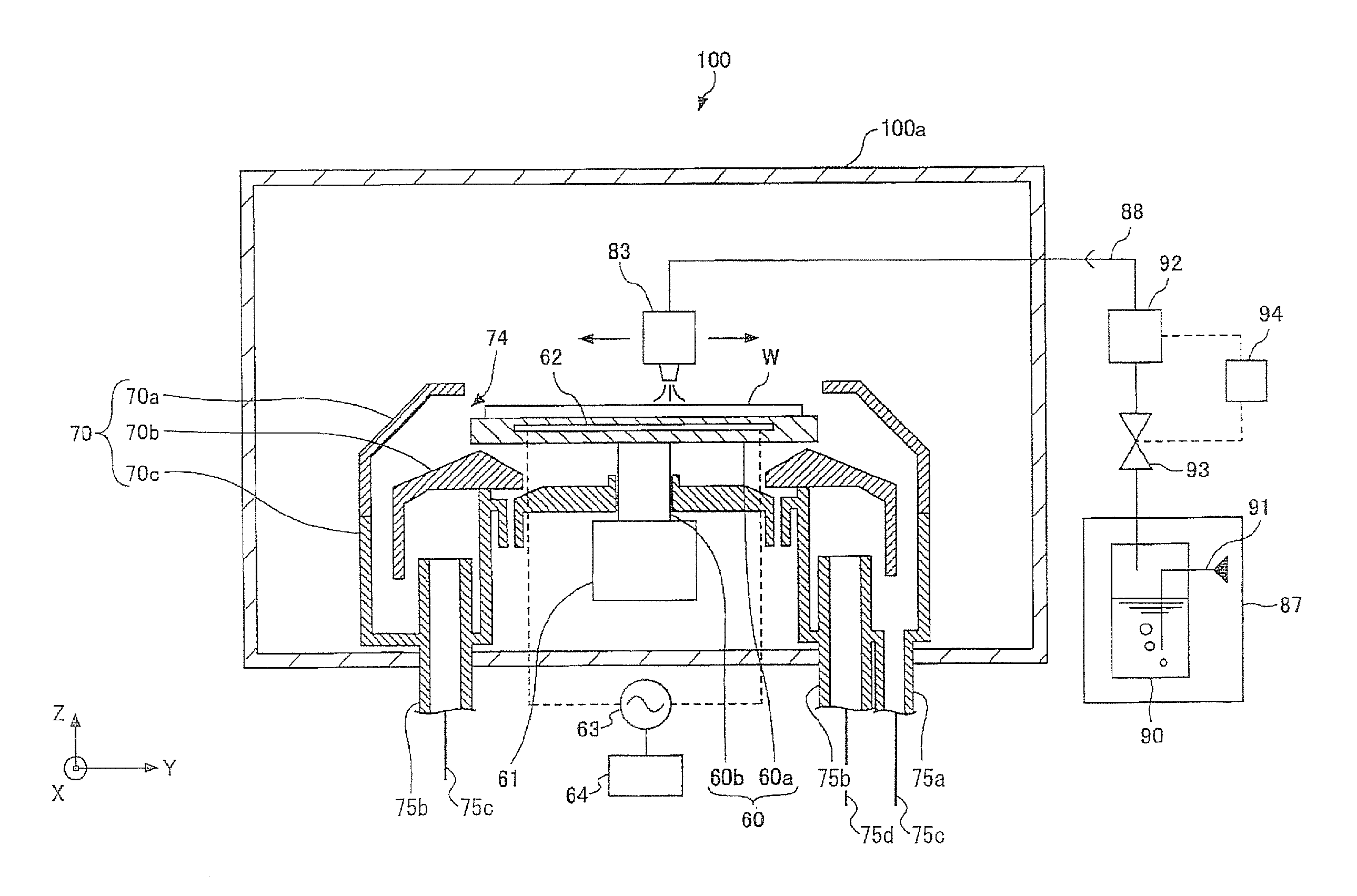
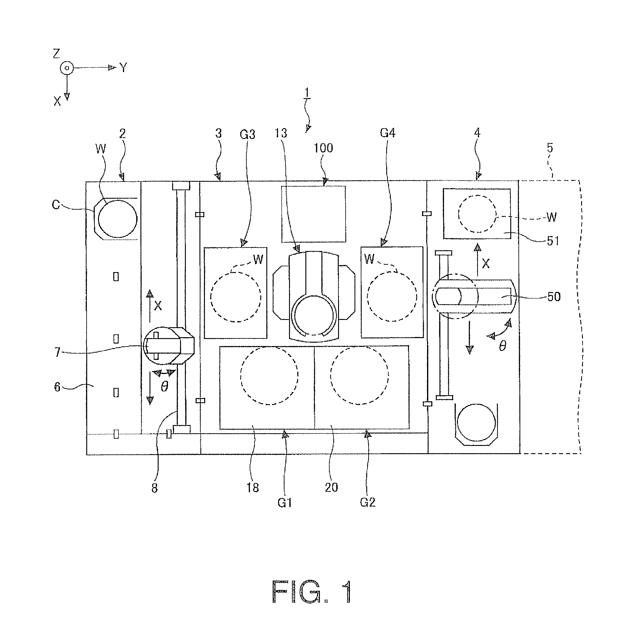
[0079]In Experiment 2, four wafers were prepared, and these wafers were subjected up to the developing process to form resist patterns thereon. At this stage, as a sample for comparison, one wafer was taken out from the resist coating and developing apparatus 1 (this wafer is referred to as “wafer a” for the matter of convenience). Then, one (referred to as “wafer b”) of the rest three wafers was transported to the resist-film processing apparatus 100 and was exposed to the solvent gas. The wafer b was taken out, without any release liquid being supplied thereto. Then, one (wafer c) of the rest two wafers was transported to the resist-film processing apparatus 100. The wafer c was exposed to the solvent gas, and the release liquid was supplied thereto. Then, the wafer c was washed with water, dried, and taken out. The last one wafer (wafer d) was transported to the resist-film processing apparatus 100. Then, the release liquid was supplied to the wafer d, without the wafer d being e...
PUM
| Property | Measurement | Unit |
|---|---|---|
| critical dimension | aaaaa | aaaaa |
| critical dimension | aaaaa | aaaaa |
| temperature | aaaaa | aaaaa |
Abstract
Description
Claims
Application Information
 - R&D
- Intellectual Property
- Life Sciences
- Materials
- Tech Scout
- Unparalleled Data Quality
- Higher Quality Content
- 60% Fewer Hallucinations
Browse by: Latest US Patents, China's latest patents, Technical Efficacy Thesaurus, Application Domain, Technology Topic, Popular Technical Reports.
© 2025 PatSnap. All rights reserved.Legal|Privacy policy|Modern Slavery Act Transparency Statement|Sitemap|About US| Contact US: help@patsnap.com


