
Light emitting device, method of driving pixel circuit, and driving circuit

a technology of light emitting devices and circuits, applied in the direction of instruments, light sources, electroluminescent light sources, etc., to achieve the effect of reducing the influence of electrical characteristics

Inactive Publication Date: 2013-05-30
SEIKO EPSON CORP
View PDF8 Cites 3 Cited by
  • Summary
  • Abstract
  • Description
  • Claims
  • Application Information

AI Technical Summary

Benefits of technology

The invention relates to a driving circuit and a light emitting device that can reduce the influence of the electrical characteristics of the light emitting element on the driving current. By setting the gate potential of the light-emission control transistor in the saturation region for the light emitting period, a change in the potential of the node between the light-emission control transistor and the driving transistor can be suppressed. This results in a reduced influence of the electrical characteristics of the light emitting element on the driving current. Additionally, the invention also provides a stable constant current source for the driving current by utilizing the driving transistor in the saturation region. Overall, this invention improves the stability and reliability of the driving circuit and the light emitting device.

Problems solved by technology

On the other hand, the electrical characteristics of each light emitting element E include errors (e.g., an error from a design value and a variation between elements).

Method used


Image

  • Light emitting device, method of driving pixel circuit, and driving circuit
  • Light emitting device, method of driving pixel circuit, and driving circuit
  • Light emitting device, method of driving pixel circuit, and driving circuit

Examples


first embodiment

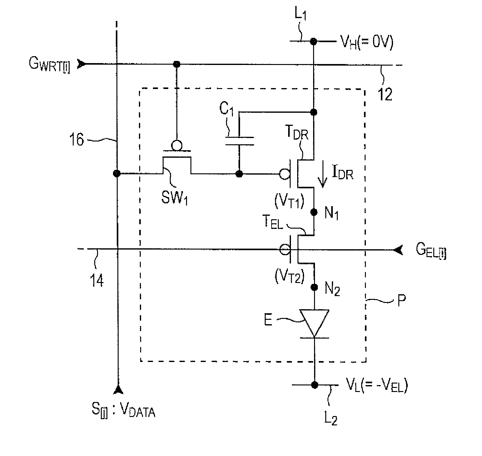
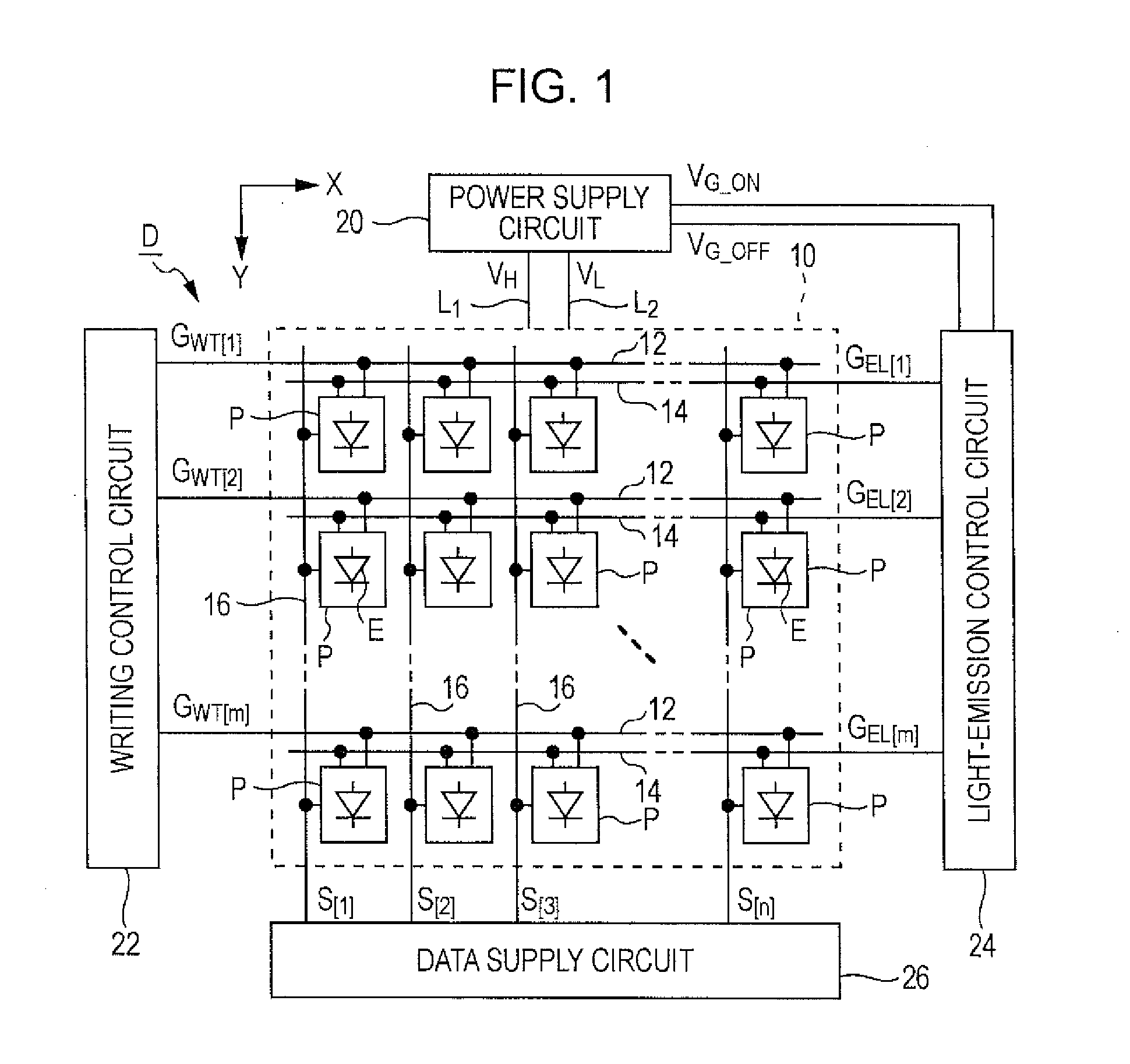
[0038]FIG. 1 is a block diagram of a light emitting device for use as an image display unit in various electronic apparatuses. A light emitting device D according to a first embodiment of the invention includes an element array 10 and peripheral circuits (i.e., a power supply circuit 20, a writing control circuit 22, a light-emission control circuit 24, and a data supply circuit 26). The element array 10 includes many pixel circuits P. The peripheral circuits control the pixel circuits P. Each pixel circuit P includes a light emitting element E which emits light by receiving a current.

[0039]In the element array 10, m selection lines 12 extending in the X direction, m light-emission control lines 14 extending in the X direction, and n data lines 16 extending in the Y direction that is perpendicular to the X direction (each of m and n is a natural number of two or more). Each light-emission control line 14 pairs with the corresponding selection line 12. Each pixel circuit P is arrange...

second embodiment

[0065]A second embodiment of the invention will now be described. Components having the same functions and operations as those of the components in the first embodiment are designated by the same reference numerals and a detail description thereof is omitted.

[0066]FIG. 8 is a circuit diagram of the structure of a pixel circuit P in the second embodiment. As shown in FIG. 8, transistors (e.g., a driving transistor TDR, a light-emission control transistor TEL, and a transistor SW1) constituting the pixel circuit P are of N-channel type. Therefore, the relationship among power supply lines L1 and L2 and components of the pixel circuit P is the reverse of that in the first embodiment. In other words, the anode of a light emitting element E is connected to the power supply line L1 and the source of the driving transistor TDR is connected to the power supply line L2. The potential VL of the power supply line L2 is a reference potential (0 V) for the voltages across respective components. ...

third embodiment

[0076]FIG. 10 is a circuit diagram of the structure of a pixel circuit P according to a third embodiment of the invention. Referring to FIG. 10, the pixel circuit P according to this embodiment includes a transistor SW2 and a capacitor C2 in addition to the same components as those in the first embodiment. The transistor SW2 is a P-channel transistor, arranged between the gate and the drain of a driving transistor TDR, for controlling the electrical connection between the gate and the drain. A control signal GCP[i] is supplied from a driving circuit (not shown) to the gate of the transistor SW2 via a control line 18. The capacitor C2 includes an electrode E1 and an electrode E2. The electrode E1 is connected to the gate of the driving transistor TDR. The transistor SW2, arranged between the electrode E2 and a data line 16, controls the electrical connection therebetween.

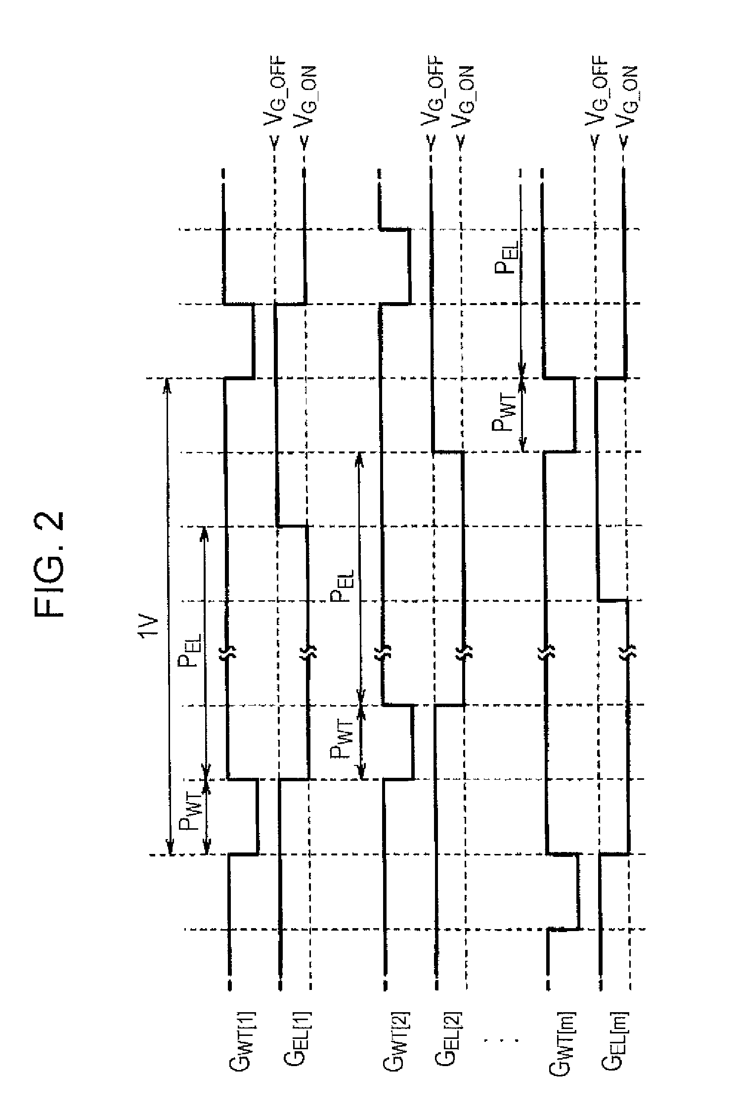
[0077]FIG. 11 is a timing chart showing the waveforms of signals supplied to the pixel circuit P at the intersecti...


PUM


Abstract

A method of driving a pixel circuit is provided. The pixel circuit includes a light emitting element that emits light by receiving a driving current, a driving transistor that generates the driving current, and a light-emission control transistor of the same conductivity type as that of the driving transistor, the light-emission control transistor being arranged on a path through which the driving current flows from the driving transistor to the light emitting element. The method includes setting the gate potential of the light-emission control transistor so that the light-emission control transistor is turned on in the saturation region for a light emitting period during which the light emitting element is allowed to emit light.

Description

[0001]This application is a U.S. Divisional of U.S. application Ser. No. 11 / 765,206 filed Jun. 19, 2007, which claims the benefit of priority to Japanese Patent Application No. 2006-183054 filed Jul. 3, 2006, the contents of which are incorporated herein by reference.BACKGROUND[0002]1. Technical Field[0003]The present invention relates to a technique of controlling a light emitting element, such as an organic light emitting diode.[0004]2. Related Art[0005]Light emitting devices using active elements, such as thin film transistors, for controlling a current (hereinafter, referred to as a driving current) supplied to a light emitting element have been proposed. FIG. 18 shows the arrangement of a driving transistor TDR and a light-emission control transistor TEL on a path through which a driving current IDR flows, the arrangement being disclosed in, for example, U.S. Pat. No. 6,229,506 and JP-A-2003-22049. The driving transistor TDR generates the driving current IDR according to the ga...

Claims


Application Information

Patent Timeline
Patent Type & Authority Applications(United States)
IPC IPC(8): H05B37/02
CPCG09G3/3233G09G3/3291G09G2300/0819H05B37/02G09G2300/0852G09G2300/0861G09G2320/043G09G2300/0842H05B47/10G09G3/20G09G3/30G09G3/32H05B33/12
Inventor NOZAWA, TOSHIYUKI
Owner SEIKO EPSON CORP
Learn More