Metal PCB having hole reflective surface and method for manufacturing the same

Inactive Publication Date: 2013-05-30
EG LITEC CO LTD
View PDF0 Cites 2 Cited by
  • Summary
  • Abstract
  • Description
  • Claims
  • Application Information

AI Technical Summary

Benefits of technology

The present invention provides a metal PCB with a hole reflective surface and a simplified method of manufacturing the same. This simplifies the manufacturing process and makes the product more usable. The method involves surface treatment on a metal plate and a process of bonding a PCB having a hole, thus reducing manufacturing costs and simplifying the process. The reflective surface formed by surface treatment on the metal plate and on the side of a hole in the PCB layer helps to increase the reflection efficiency of light, thus reducing the manufacturing process. The technical effects of this invention include reducing complexity, simplifying the manufacturing process, and increasing reflection efficiency of LED products.

Problems solved by technology

The reason for this is that dislocation and mismatch occur in a crystalline structure of the LED chip when the heat generated from the LED chip remains in the LED chip for a long time.
The high power LED is operated by high voltage power, and thus a large amount of heat is generated from an LED chip by the high voltage power.
However, the LED package of the prior art does not comprise a lead structure for electrically connecting the LED chip to external electrodes, and thus it is difficult to mount the LED package on a typically used PCB.
This manufacturing process of the LED products according to the prior art is a complex multi-stage process involving various manufacturers, and thus it is difficult to maintain quality control.
Moreover, there are many limiting factors in manufacturing the high-efficiency LED products such as formation of reflective surfaces, etc., which is problematic.
In the process of manufacturing the metal PCBs according to the prior art, a method of plating the surface of the metal plate is used to form a first reflective structure, which results in an increase in manufacturing costs.
Moreover, in the case where a reflective surface in the form of a cup is formed to form a second reflective structure, the LED chip is bonded to a position lower than the surface of the metal plate, which increases the complexity of its connection to a circuit pattern, for example.
In this case, there is a problem of heat dissipation due to the presence of the adhesive layer in the area where the LED chip is located.
In this case, the manufacturing costs are further increased, and the dam structure is not uniform, thus affecting the color temperature.

Method used


Image

  • Metal PCB having hole reflective surface and method for manufacturing the same
  • Metal PCB having hole reflective surface and method for manufacturing the same
  • Metal PCB having hole reflective surface and method for manufacturing the same

Examples


Embodiment Construction

[0046]Hereinafter, preferred embodiments of a metal PCB having a hole reflective surface and a method for manufacturing the same according to the present invention will be described in detail with reference to the accompanying drawings.

[0047]Features and advantages of the metal PCB having a hole reflective surface and the method for manufacturing the same according to the present invention will be apparent from the following detailed description of the preferred embodiment of the present invention.

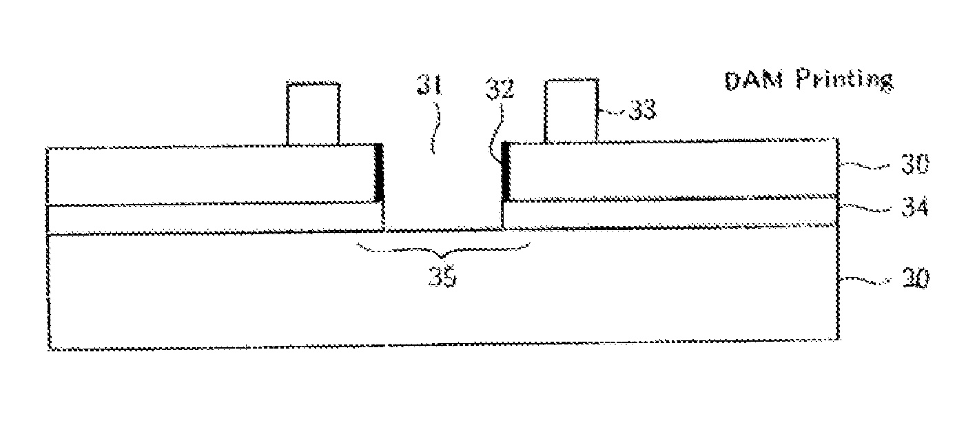
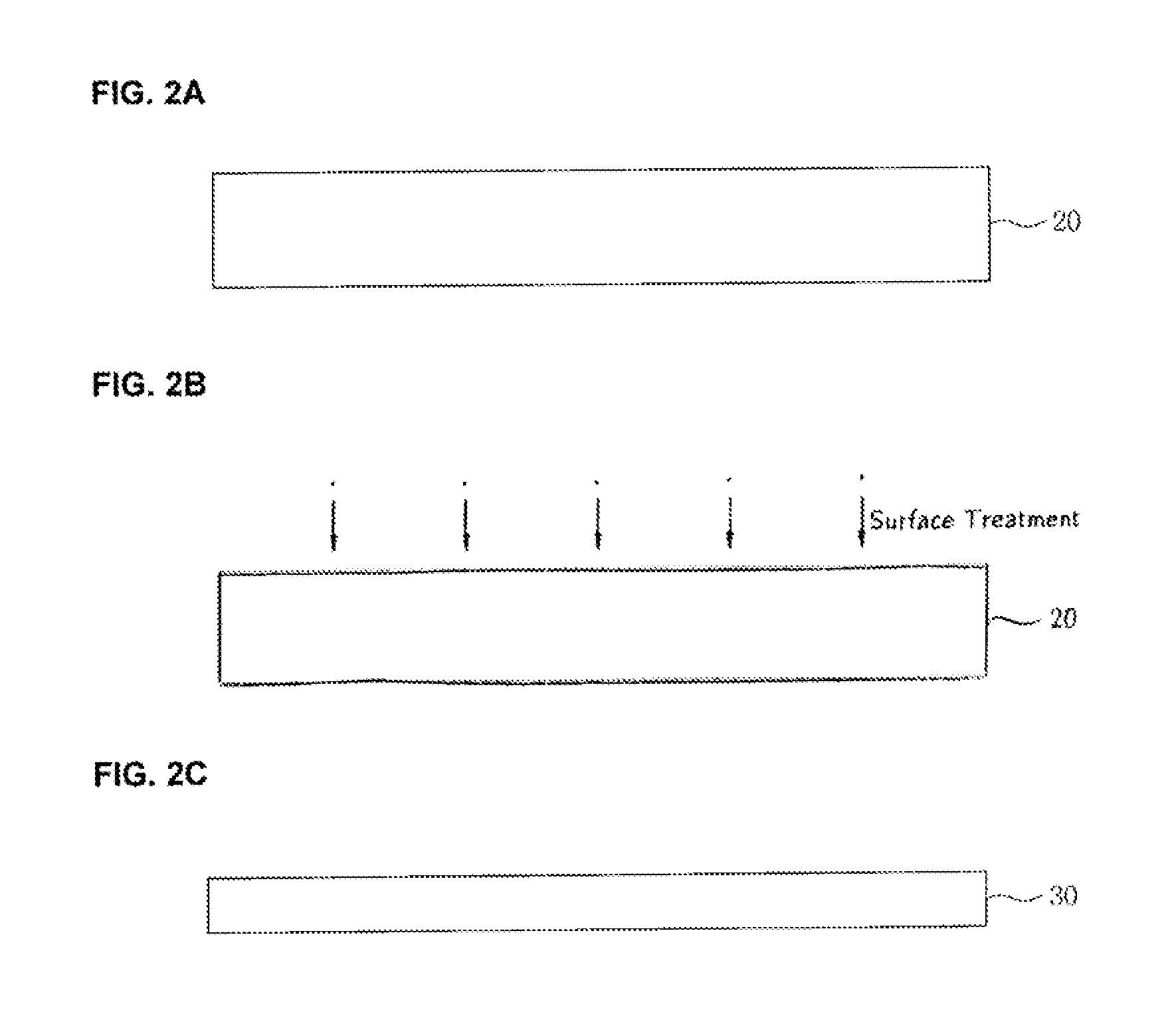
[0048]FIGS. 2A to 2G are cross-sectional views showing a process of manufacturing a metal PCB having a hole reflective surface according to the present invention.

[0049]The present invention provides a metal PCB having a hole reflective surface and a method for manufacturing the same, in which a process of forming a first reflective structure is achieved by performing surface treatment such as chemical polishing, etc. on a metal plate, instead of a high cost process such as plating, etc. an...


PUM

PropertyMeasurementUnit
Heightaaaaaaaaaa
Areaaaaaaaaaaa
Reflectionaaaaaaaaaa

Abstract

A metal printed circuit board (PCB) having a hole reflective surface and a method for manufacturing the same, in which a process of forming a reflective surface by performing surface treatment on a metal plate and a process of bonding a PCB having a hole are performed as a single process, thus simplifying the manufacturing process and increasing the applicability of a product. The metal PCB includes a metal plate having a first reflective surface formed on a chip bonding area by surface treatment; a PCB layer stacked on the metal plate and having a hole and a wiring pattern which are formed in the chip bonding area; a second reflective surface formed on the inner side of the hole of the PCB layer; and a dam formed around the hole on the PCB layer.

Description

CROSS-REFERENCE TO RELATED PATENT APPLICATION[0001]This application claims the benefit of Korean Patent Application No. 10-2011-0126095, filed on Nov. 29, 2011, in the Korean Intellectual Property Office, the disclosure of which is incorporated herein in its entirety by reference.BACKGROUND OF THE INVENTION[0002]1. Field of the Invention[0003]The present invention relates to a metal printed circuit board (PCB) and, more particularly, to a metal PCB having a hole reflective surface and a method for manufacturing the same, in which a process of forming a reflective surface by performing surface treatment on a metal plate and a process of bonding a PCB having a hole are performed as a single process, thus simplifying the manufacturing process and increasing the applicability of a product.[0004]2. Description of the Related Art[0005]In general, a light emitting diode (LED) is a device that emits light by recombination of electrons and holes at a P-N junction upon application of an elect...

Claims


Application Information

Patent Timeline
IPC IPC(8): H05K3/00H05K1/03
CPCH01L33/60H01L33/64H05K3/0061Y10T29/49124H05K2201/10106H05K2201/2054H05K2201/09027H01L2224/48091H01L2224/48227H01L2924/00014
Inventor JANG, JONG-JIN
Owner EG LITEC CO LTD
Why Eureka
Try Eureka