
Surface mount technology process for advanced quad flat no-lead package process and stencil used therewith

a technology of surface mount and stencil, which is applied in the direction of final product manufacturing, sustainable manufacturing/processing, and semiconductor/solid-state device details

Inactive Publication Date: 2013-05-30
MEDIATEK SINGAPORE PTE LTD SINGAPORE
View PDF7 Cites 9 Cited by
  • Summary
  • Abstract
  • Description
  • Claims
  • Application Information

AI Technical Summary

Benefits of technology

The present invention is about a process for making a special semiconductor package. This invention is about how to join together the different parts of the package using solder. The invention is particularly useful for a specific type of package called an advanced quad flat no-lead package. This invention helps to improve the quality and reliability of the solder joint in this package design.

Problems solved by technology

However, the process reliability of surface mounting of the aQFN package to a printed circuit board (PCB) suffers from the stress of solder joints between the die pad / leads of the aQFN package and the PCB, leading to a solder joint cracking problem.

Method used


Image

  • Surface mount technology process for advanced quad flat no-lead package process and stencil used therewith
  • Surface mount technology process for advanced quad flat no-lead package process and stencil used therewith
  • Surface mount technology process for advanced quad flat no-lead package process and stencil used therewith

Examples


Embodiment Construction

[0016]The following description is a mode for carrying out the invention. This description is made for the purpose of illustrating the general principles of the invention and should not be taken in a limiting sense. The scope of the invention is best determined by reference to the appended claims. Wherever possible, the same reference numbers are used in the drawings and the descriptions to refer the same or like parts.

[0017]The present invention will be described with respect to particular embodiments and with reference to certain drawings, but the invention is not limited thereto and is only limited by the claims. The drawings described are only schematic and are non-limiting. In the drawings, the size of some of the elements may be exaggerated and not drawn to scale for illustrative purposes. The dimensions and the relative dimensions do not correspond to actual dimensions to practice of the invention.

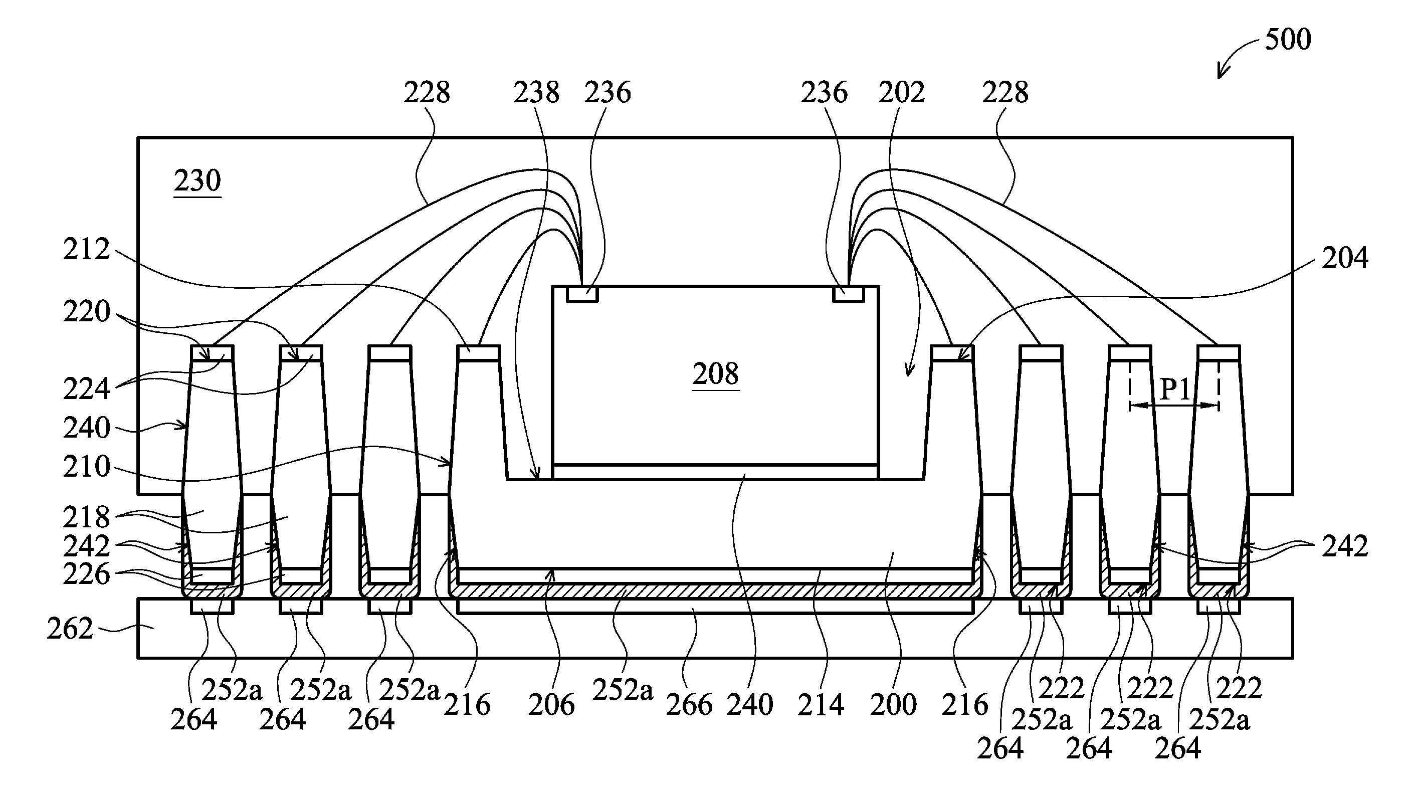
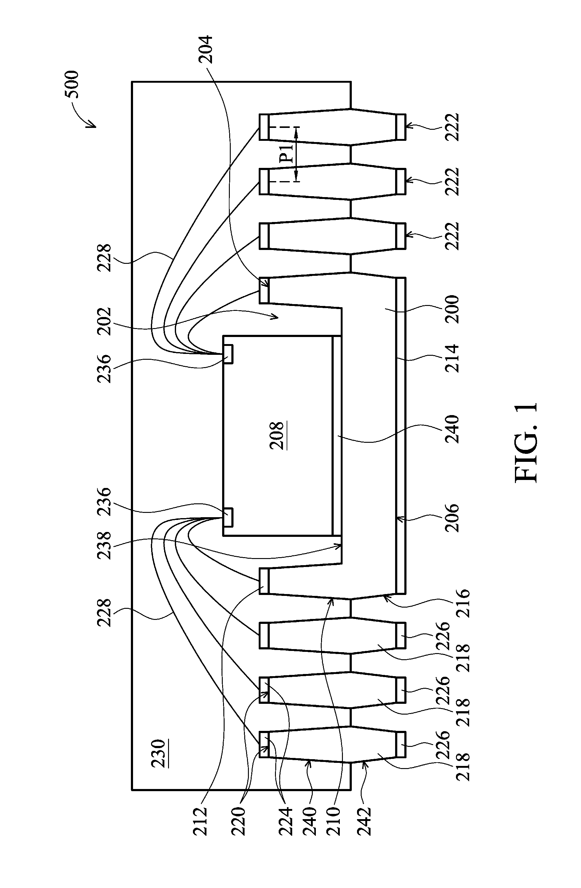
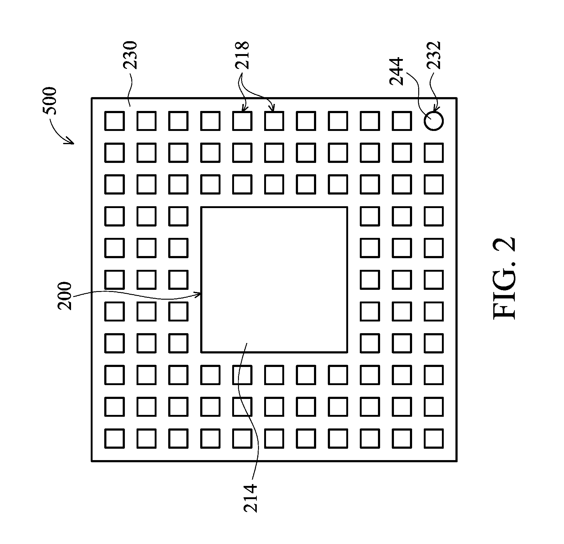
[0018]FIG. 1 shows a side view of one exemplary embodiment of an advanced quad ...


PUM

PropertyMeasurementUnit
area ratioaaaaaaaaaa
thermalaaaaaaaaaa
electrical performanceaaaaaaaaaa

Abstract

The invention provides a surface mount technology process for an advanced quad flat no-lead package process and a stencil used therewith. The surface mount technology process for an advanced quad flat no-lead package includes providing a printed circuit board. A stencil with first openings is mounted over the printed circuit board. A solder paste is printed passing the first openings to form first solder paste patterns. The stencil is taken off. A component placement process is performed to place the advanced quad flat no-lead package comprising a die pad on the printed circuit board, wherein the first solder paste patterns contact a lower surface of the die pad, and an area ratio of the first openings to the lower surface of the die pad is between 1:2 and 1:10. A reflow process is performed to melt the first solder paste patterns to surround a sidewall of the die pad.

Description

BACKGROUND OF THE INVENTION[0001]1. Field of the Invention[0002]The present invention relates to a surface mount technology process for an advanced quad flat no-lead package process and a stencil used therewith, and in particular, to a solder joint design for a die pad of an advanced quad flat no-lead package.[0003]2. Description of the Related Art[0004]An advanced quad flat no-lead (aQFN) package is a leadless, multi-row and fine pitch lead frame package with advantages of having a low profile, small footprint, light weight and free-form I / O design, thereby having enhanced thermal and electrical performance. The aQFN package can be used as a high-volume cost-sensitive consumer application in, for example, telecommunication products, portable products, consumer products and medium lead count packages. Also, the aQFN package has a significant cost benefit be replacing Au wire with Cu wire. Therefore, the aQFN package can increase cost competitiveness with low wire costs.[0005]However...

Claims


Application Information

Patent Timeline
Patent Type & Authority Applications(United States)
IPC IPC(8): H05K3/34H05K3/12
CPCH01L2224/45144H05K1/111H05K2201/10803H01L23/49503H01L23/49548H01L23/49582H01L24/29H01L24/32H01L24/45H01L2224/2919Y10T29/53174H05K2201/10969H05K3/3484H05K3/3436H01L2224/48091H01L2224/73265H01L2224/48247H01L2224/32245H01L2224/32257H01L2224/48257H01L24/48H05K3/1225H05K2201/09427Y10T29/49144H01L2224/45147H01L2924/00015H01L2924/00014H01L2924/00012H01L2924/00H01L24/73H01L2924/181H05K3/3485Y02P70/50
Inventor HSU, CHIH-TAICHEN, NAN-CHENGCHIANG, CHIH-MINGHUNG, HUNG-CHANGZHONG, XIN
Owner MEDIATEK SINGAPORE PTE LTD SINGAPORE
Learn More