Piezoelectric device of polymer
a polymer and polymer technology, applied in the direction of device material selection, material nanotechnology, piezoelectric/electrostrictive device material selection, etc., can solve the problems of low dielectric constant and electro-mechanical coupling coefficient, inability to obtain sufficient performance, and various limitations in usag
- Summary
- Abstract
- Description
- Claims
- Application Information
AI Technical Summary
Benefits of technology
Problems solved by technology
Method used
Image
Examples
embodiment 1
[0049]After the polyvinylidene florodide-trifluoroethylene (PVDF-TrFE) is solved in a methyl ethyl ketone solvent, it is coated on a base film by being casted. The polyvinylidene florodide-trifluoroethylene (PVDF-TrFE) is obtained in a shape of film by evaporating the solvent.
[0050]The first electrodes are formed in a thickness of 0.1 μm by forming the graphene composites electrodes (graphene+is a silver nano wire) on both surfaces of the polyvinylidene florodide-trifluoroethylene (PVDF-TrFE) with a slot die coating method.
[0051]The second electrodes in the shape of a transparent grid are formed in a thickness of 0.1 μm by forming the silver nano wire electrodes on both surfaces of the first electrodes with the slot die coating method.
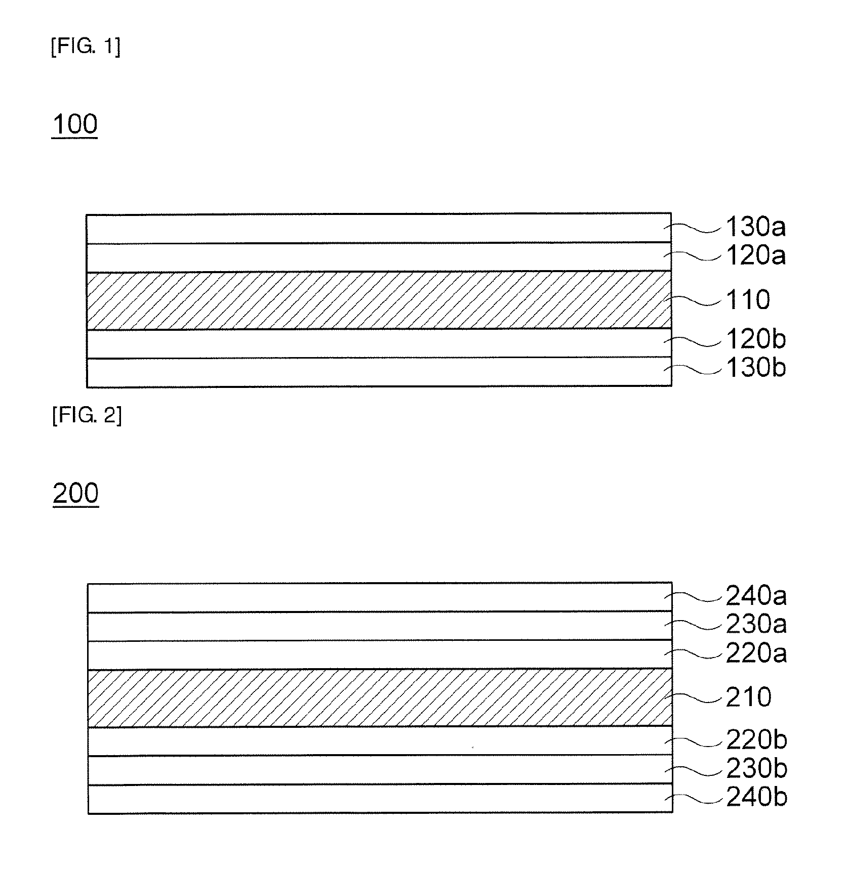
[0052]The piezoelectric device finally manufactured in accordance with the embodiment 1 makes to have the structure of the following FIG. 1.
embodiment 2
[0053]After the polyvinylidene florodide-trifluoroethylene (PVDF-TrFE) is solved in a methyl ethyl ketone solvent, it is coated on a base film by being casted. The polyvinylidene florodide-trifluoroethylene (PVDF-TrFE) is obtained in a shape of film by evaporating the solvent.
[0054]The first electrodes are formed in a thickness of 0.1 μm by forming the graphene composites electrodes (graphene+is a silver nano wire) on both surfaces of the polyvinylidene florodide-trifluoroethylene (PVDF-TrFE) with a slot die coating method.
[0055]The second electrodes in the shape of a transparent grid are formed in a thickness of 0.1 μm by forming the silver nano wire electrodes on both surfaces of the first electrodes with the slot die coating method.
[0056]The third electrodes are formed in a thickness of 0.1 μm by forming the graphene composites (graphene+conductive polymer) electrodes on both surfaces of the second electrodes with a gravure coating method.
[0057]The piezoelectric device finally ma...
PUM
| Property | Measurement | Unit |
|---|---|---|
| thicknesses | aaaaa | aaaaa |
| thickness | aaaaa | aaaaa |
| structure | aaaaa | aaaaa |
Abstract
Description
Claims
Application Information
 - R&D
- Intellectual Property
- Life Sciences
- Materials
- Tech Scout
- Unparalleled Data Quality
- Higher Quality Content
- 60% Fewer Hallucinations
Browse by: Latest US Patents, China's latest patents, Technical Efficacy Thesaurus, Application Domain, Technology Topic, Popular Technical Reports.
© 2025 PatSnap. All rights reserved.Legal|Privacy policy|Modern Slavery Act Transparency Statement|Sitemap|About US| Contact US: help@patsnap.com


