Stack-up structure of an optical panel and manufacturing method thereof
- Summary
- Abstract
- Description
- Claims
- Application Information
AI Technical Summary
Benefits of technology
Problems solved by technology
Method used
Image
Examples
Embodiment Construction
[0021]In order to make those skilled in the art have better understanding of the present disclosure, the following context particularly takes the favorable embodiment of the present disclosure, coupled with attached schema for detailed illustration for the constituent content of the present disclosure and the efficiency to be attained.
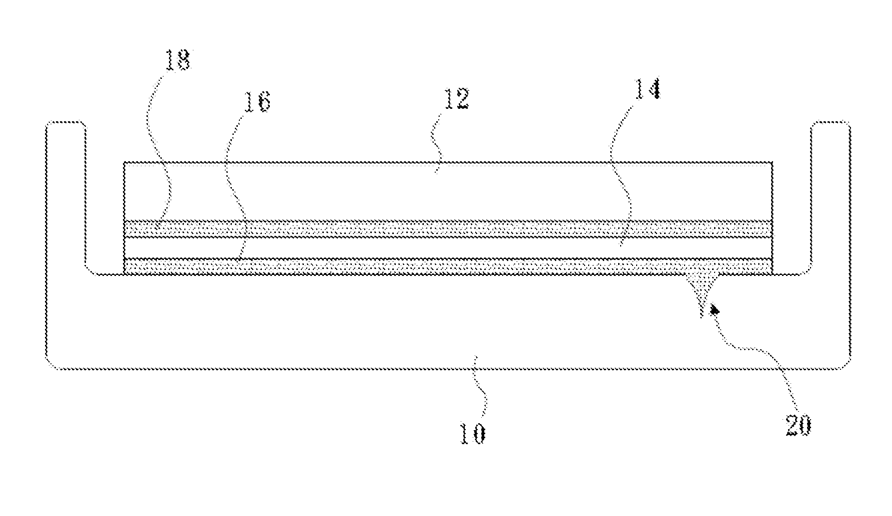
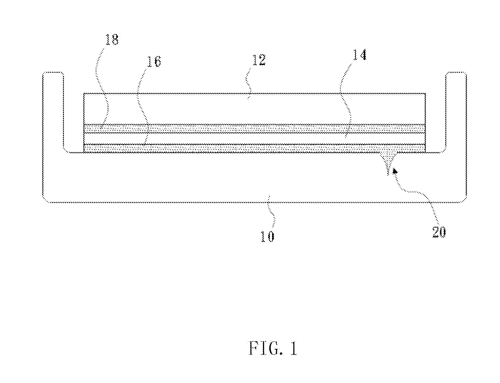
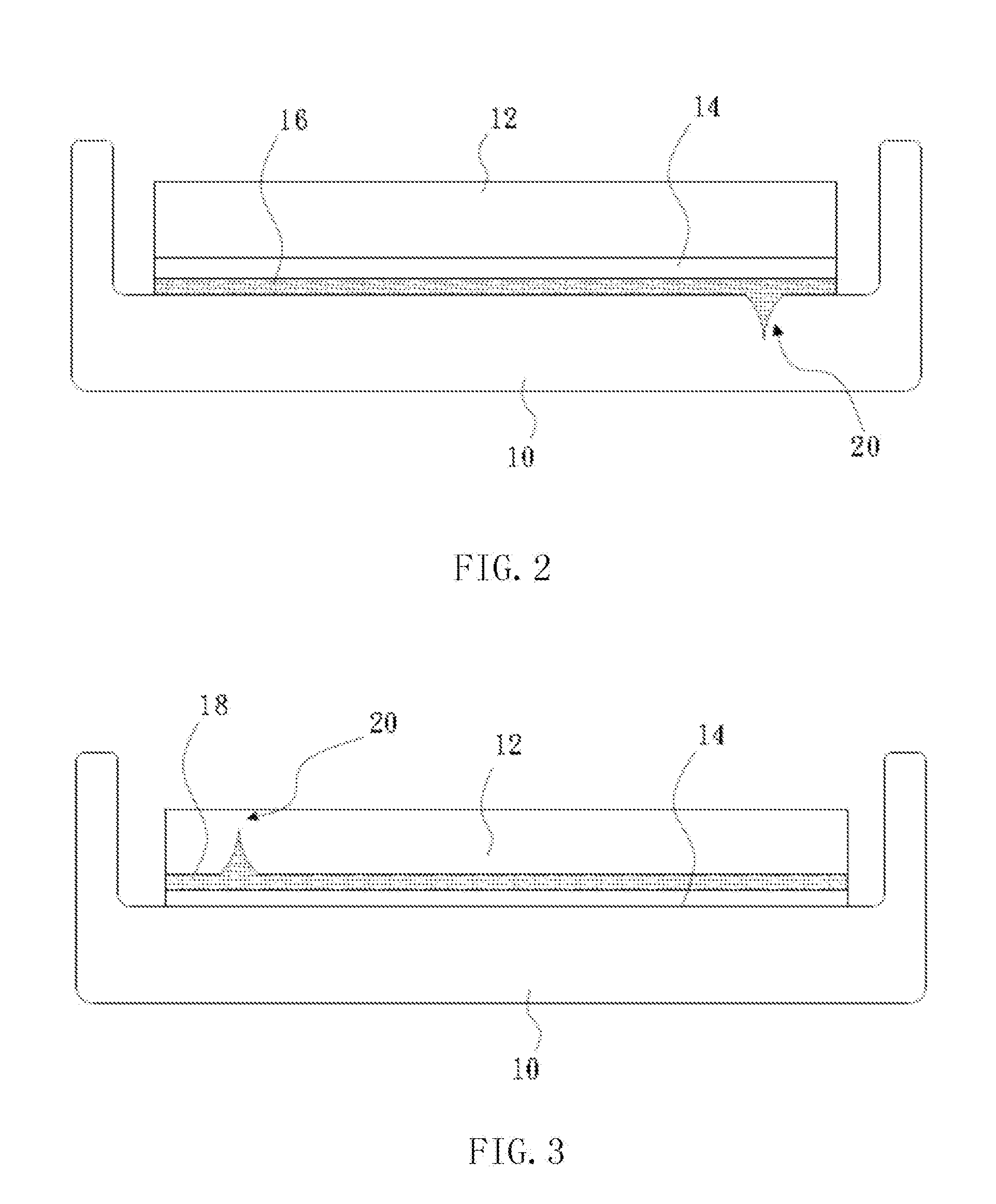
[0022]A stack-up structure of an optical panel shown in FIG. 1 comprises: a first laminating element 10, a second laminating element 12 and an adhesive layer 14. A first protective layer 16 is formed on a laminating face, which is opposite to the adhesive layer 14 of the first laminating element 10, and a second protective layer 18 is formed on the laminating face which is opposite to the adhesive layer 14 of the second laminating element 12. The first protective layer 16 is used for flattening the laminating face of the first laminating element 10 and the second protective layer 18 is used for flattening the laminating face of the second laminating el...
PUM
| Property | Measurement | Unit |
|---|---|---|
| Adhesivity | aaaaa | aaaaa |
Abstract
Description
Claims
Application Information
 - R&D
- Intellectual Property
- Life Sciences
- Materials
- Tech Scout
- Unparalleled Data Quality
- Higher Quality Content
- 60% Fewer Hallucinations
Browse by: Latest US Patents, China's latest patents, Technical Efficacy Thesaurus, Application Domain, Technology Topic, Popular Technical Reports.
© 2025 PatSnap. All rights reserved.Legal|Privacy policy|Modern Slavery Act Transparency Statement|Sitemap|About US| Contact US: help@patsnap.com


