Photovoltaic UV detector

a technology of photovoltaic uv and detector, applied in the field of photovoltaic uv detector, can solve the problems of skin cancer, cataracts, solar retinitis and corneal dystrophies, and the performance of silicon uv detectors under strong uv irradiation often deteriorates

Inactive Publication Date: 2013-01-31
AGENCY FOR SCI TECH & RES
View PDF0 Cites 21 Cited by
  • Summary
  • Abstract
  • Description
  • Claims
  • Application Information

AI Technical Summary

Problems solved by technology

UV irradiation from sunlight has also been found to be a major cause of skin cancer, tanning, eye cataracts, solar retinitis and corneal dystrophies.
(1) As the most commonly used semiconductor material for UV detectors, silicon is not stable under intensive UV irradiation over a long period of time. Consequently, performance of silicon UV detectors under strong UV irradiation often deteriorates over a long irradiation time. Most metals typically used in UV detectors are also unstable under continuous UV irradiation in air. For the metal-semiconductor Schottky UV detector 20, the metal layer 23 is directly exposed to the incident UV light 11, and any material instability can lead to serious deterioration of the photovoltaic UV detector 20 performance. In addition, metal 23 often has poor transparency for UV light. For example, UV light transmission for a polycrystalline Au layer 23 with a thickness of 100 nm is less than 1%.
(2) The magnitude of the photovoltaic output voltage (called photovoltage) is limited by the height of the energy barrier at the interface, which would be the Schottky junction 29 between the metal 23 and the semiconductor material 24, or at the p-n junction 12 for the photovoltaic UV detector 10 using two semiconductors 13 and 14. For both the Schottky junction 29 and the p-n junction 12, the internal electric field 25, 15 that separates the electrons 26, 16 and holes 27,17 only exists at the space charge region 22, 12 of the interface. There is no electric field in the bulk region of the semiconductor 24, 14, 13 outside the space charge region 22, 12.

Method used


Image

  • Photovoltaic UV detector
  • Photovoltaic UV detector
  • Photovoltaic UV detector

Examples


Embodiment Construction

[0055]Preferred embodiments of a photovoltaic UV detector according to the present invention will now be described with reference to FIGS. 3 to 9.

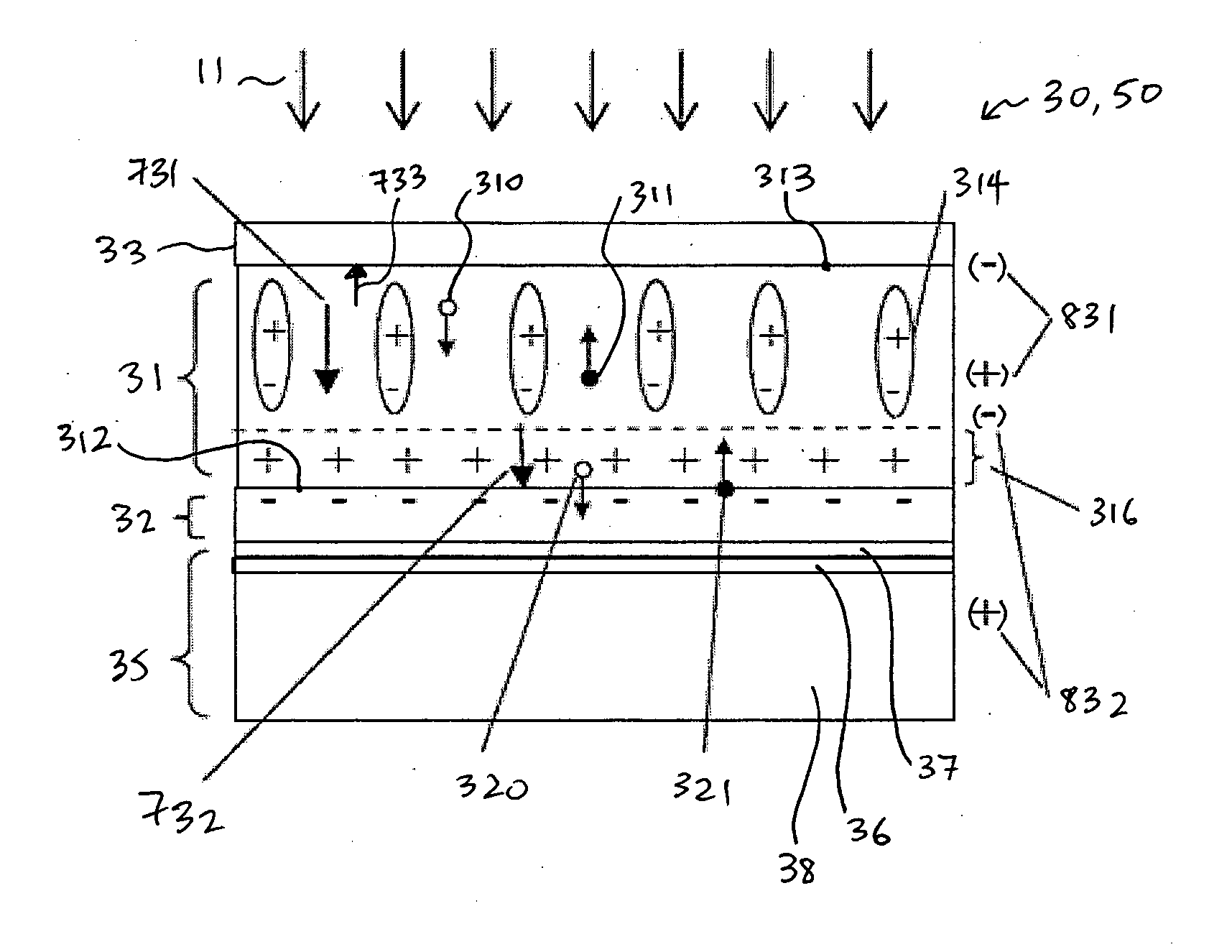
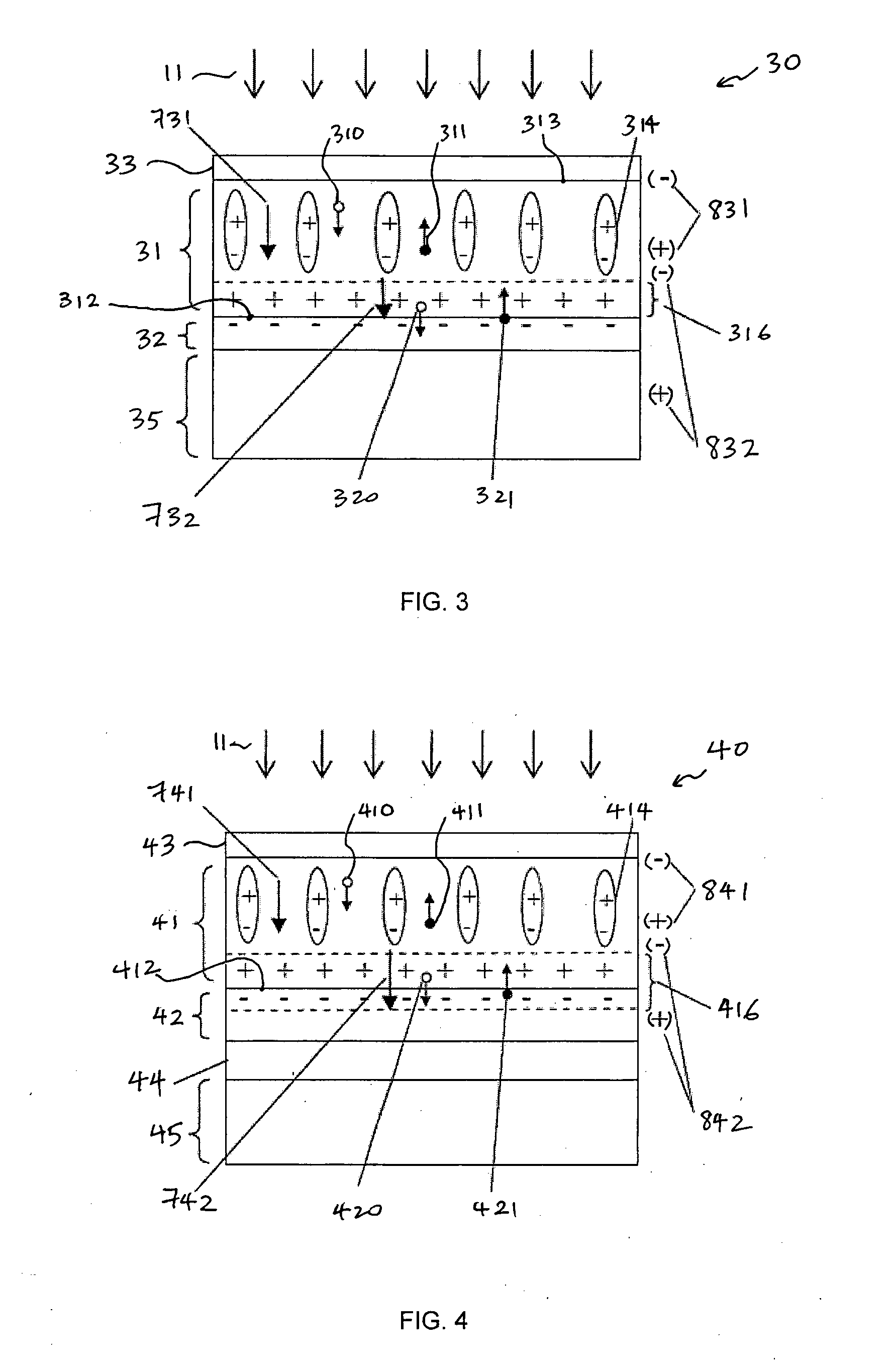
[0056]FIG. 3 shows a photovoltaic UV detector 30 with electrical output generated under UV irradiation 11 according to a first exemplary embodiment. The photovoltaic UV detector 30 has a multilayer structure. A first layer 31 comprises an electrically polarized dielectric thin layer configured to generate a first electrical output 831 under the UV irradiation 11. A dielectric material is an electrically insulating material with a large electric impedance. Preferably, the electrically polarized dielectric thin layer 31 is a ferroelectric thin film 31 with an oxide composition which is stable in air under UV irradiation. Thus, a first electric field 731 already exists or is comprised in a bulk region of the ferroelectric thin layer 31. Electrons rather than holes are the majority charge carriers in the ferroelectric thin layer 31, and so the...


PUM


Abstract

A photovoltaic UV detector configured to generate an electrical output under UV irradiation. The photovoltaic UV detector comprises a first layer comprising an electrically polarized dielectric thin layer configured to generate a first electrical output under the UV irradiation; and a second, layer configured to form an electrical energy barrier at an interface between the second layer and the first layer so as to generate a second electrical output under the UV irradiation, the second electrical output having a same polarity as the first electrical output, the electrical output of the photovoltaic UV detector being a sum of at least the first electrical output and the second electrical output. The electrically polarized dielectric thin layer may be a ferroelectric thin film, which may comprise PZT or PZLT. The second layer may be a metal and the electrical energy barrier may be a Schottky barrier.

Description

TECHNICAL FIELD[0001]The present invention relates to photovoltaic UV detectors.BACKGROUND[0002]Ultraviolet (UV) rays generate pronounced effects on many things, including material structures and properties, chemical reactions, micro-organisms, and other living things. Ultraviolet (UV) irradiation has been widely used in many applications such as materials processing, sterilization, and medical treatment. In these applications, UV intensity has to be carefully controlled, resulting in a need for UV intensity monitoring and dosage measurement.[0003]UV irradiation from sunlight has also been found to be a major cause of skin cancer, tanning, eye cataracts, solar retinitis and corneal dystrophies. However, a small amount of UV is beneficial and even essential for the production of vitamin D in human beings. In addition, because of the variability of skin type and health condition between individuals, UV exposure levels that may cause significant damage to one person may be benign and e...

Claims


Application Information

Patent Timeline
Patent Type & Authority Applications(United States)
IPC IPC(8): H01L31/101H01L31/11H01L31/18H01L31/108H01L31/102
CPCH01L31/108H01L31/022466
Inventor YAO, KUIGAN, BEE KEENLAI, SZU CHENG
Owner AGENCY FOR SCI TECH & RES
Why Eureka
Try Eureka